
Back to blog
Lead vs Lead-Free Soldering and Solder Melting Points in PCB

solder melting point
The global electronics industry is undergoing a significant transformation towards environmentally sustainable practices. One critical aspect of this shift is the move from traditional lead-based soldering to lead-free soldering in Printed Circuit Board Assembly (PCBA). Understanding the nuances between these two soldering methods is essential for ensuring the reliability, performance, and environmental compliance of electronic products. This comprehensive article delves into the technical aspects, challenges, and practical considerations of both soldering techniques, providing valuable insights for professionals in the PCB industry.
The Importance of Solder Joints
Solder joints are the backbone of electronic assemblies, establishing both mechanical and electrical connections between components and PCBs. The integrity of these joints is crucial; even a single defective solder joint can compromise the functionality of the entire electronic device. Therefore, understanding the properties and behavior of different solder types is vital for achieving high reliability in electronic manufacturing.
Traditional Lead Soldering
Composition and Properties of Lead-Based Solder
Lead-based solder, commonly a tin-lead (SnPb) alloy, has been the industry standard for decades. The most widely used formulation, Sn37Pb, offers several advantageous properties:
- Melting Point: The eutectic composition of Sn37Pb melts at a relatively low temperature of 183°C.
- Wettability: Excellent wettability ensures robust and reliable solder joints.
- Mechanical Properties: Lead solder is relatively soft, providing good shock absorption and stress distribution.
Advantages of Lead-Based Soldering
The primary benefits of using lead solder include:
- Low Melting Point: Facilitates easier and less energy-intensive soldering processes.
- Superior Wettability: Ensures strong adhesion between components and PCBs.
- Reliable Mechanical Performance: Softness of the solder helps absorb mechanical stresses, enhancing joint durability.
Health and Environmental Risks
Despite its technical advantages, lead is highly toxic, posing significant health risks to workers and environmental hazards. This has led to stringent regulations and a global push towards eliminating lead from electronic assemblies.

solder melting point
Lead-Free Soldering
Composition and Properties of Lead-Free Solder
Lead-free solder alloys, primarily composed of tin-silver-copper (SAC) formulations like SAC305 (96.5% Sn, 3.0% Ag, 0.5% Cu), have emerged as the environmentally friendly alternative. Key properties include:
- Melting Point: SAC305 melts at approximately 217°C, higher than lead-based solder.
- Wettability: Generally poorer than lead solder, necessitating more active fluxes.
- Mechanical Properties: Lead-free solder joints tend to be harder and more brittle.
Challenges of Lead-Free Soldering
Switching to lead-free soldering introduces several challenges:
- Higher Melting Point: Requires higher processing temperatures, increasing thermal stress on components and PCBs.
- Brittleness: Lead-free solder joints are more prone to cracking and fatigue, especially under thermal cycling conditions.
- Wettability Issues: Poorer wettability can lead to incomplete or weak joints, requiring precise control of soldering parameters.
Comprehensive Comparison Between Lead and Lead-Free Soldering
Melting Point and Thermal Stress
The shift from lead-based to lead-free soldering involves significant changes in the thermal profile of the soldering process. Lead-free solders, such as those based on tin-silver-copper (SAC) alloys, have higher melting points (around 217°C) compared to traditional tin-lead (SnPb) solder (183°C). This higher melting point increases the thermal load during assembly, leading to several potential issues:
- Warping: The higher temperature can cause the PCB substrate to warp, especially if it is not uniformly heated.
- Delamination: The layers of the PCB can separate under the stress of higher temperatures.
- Component Damage: Sensitive components may not withstand the higher reflow temperatures required for lead-free soldering.
To mitigate these risks, careful thermal management is essential. This includes optimizing the reflow profile to ensure even heating, using preheating stages to reduce thermal shock, and selecting materials with higher thermal stability.
Mechanical Reliability
Mechanical reliability is a crucial factor in solder joint performance. Lead-free solder joints are typically harder and more brittle compared to their lead-based counterparts. This difference in mechanical properties has several implications:
- Cracking: The brittleness of lead-free solders makes them more prone to cracking under mechanical stress.
- Fatigue: Repeated thermal cycling, common in automotive and aerospace electronics, can lead to fatigue failures in lead-free solder joints.
Addressing these challenges requires specific strategies, such as:
- Alloy Selection: Using alloys with minor additions of elements like bismuth or nickel can improve the mechanical properties of lead-free solders.
- Joint Design: Designing solder joints to distribute stress more evenly and reduce concentration points.
- Reinforcement Techniques: Applying underfill or other reinforcement methods to support the solder joints and enhance their durability.
Wettability and Joint Formation
Wettability is a critical property that affects the formation and reliability of solder joints. Lead-based solders exhibit excellent wettability, forming strong and reliable joints with minimal effort. In contrast, lead-free solders often suffer from inferior wettability, leading to potential issues:
- Incomplete Wetting: Poor wettability can result in incomplete coverage of the pad, leading to weak joints.
- Voiding: Entrapped air or flux residues can create voids within the solder joint, compromising its mechanical and electrical integrity.
To ensure high-quality joint formation with lead-free solders, several strategies can be employed:
- Active Fluxes: Using more active flux formulations that promote better wetting and reduce oxidation.
- Optimized Soldering Parameters: Adjusting the soldering temperature, time, and atmosphere to enhance wettability.
- Surface Preparation: Ensuring that the surfaces to be soldered are clean and free of oxides.
Environmental and Health Impact
The primary motivation for transitioning to lead-free soldering is the significant reduction in environmental and health hazards associated with lead exposure. Lead is a toxic substance that poses severe risks to human health and the environment, leading to stringent regulations like the Restriction of Hazardous Substances (RoHS) directive. Lead-free soldering offers several benefits in this regard:
- Reduced Toxicity: Eliminating lead from the soldering process significantly reduces the exposure risk to workers and minimizes environmental contamination.
- Regulatory Compliance: Adopting lead-free soldering practices ensures compliance with global environmental regulations.
However, lead-free soldering is not without its trade-offs. The higher processing temperatures required for lead-free solders increase energy consumption, which can impact the overall environmental footprint. To balance these concerns, manufacturers can implement energy-efficient practices, such as:
- Efficient Thermal Management: Optimizing reflow ovens and other heating equipment to reduce energy usage.
- Advanced Materials: Developing and using materials that enable lower-temperature lead-free soldering processes.
- Recycling and Waste Management: Enhancing recycling efforts and managing waste to minimize environmental impact.
Detailed Comparison of Physical Characteristics
To illustrate the differences between lead and lead-free soldering, here is a detailed comparison of their physical properties:

Detailed Comparison of Physical Characteristics
Challenges in Lead-Free Soldering
Oxidation
Higher soldering temperatures increase the risk of oxidation, which can degrade the quality of solder joints. This challenge necessitates better flux formulations and controlled soldering environments to maintain joint integrity.
Component Compatibility
Some components, particularly those with plastic packages or electrolytic capacitors, may not withstand the higher temperatures required for lead-free soldering. Careful selection of components and potential design adjustments are necessary to ensure compatibility.
Tin Whiskers
Lead-free solders, especially those with high tin content, are prone to tin whisker growth, which can cause electrical shorts. Mitigation strategies include using barrier layers like nickel and selecting appropriate alloy compositions.
Conductive Anodic Filament (CAF)
Lead-free soldering can exacerbate the formation of CAF in PCBs, leading to short circuits and failures. Stringent material and process controls are essential to prevent this issue, particularly in high-density assemblies.
Practical Considerations for Transitioning to Lead-Free Soldering
Process Adjustment
Transitioning to lead-free soldering requires adjustments in soldering temperatures, time profiles, and equipment calibration to accommodate the higher melting points and different flow characteristics of lead-free alloys.
Material Selection
Choosing the right materials is crucial. Components must be able to withstand higher temperatures, and PCBs should have appropriate Tg (glass transition temperature) values. This ensures the assembly can endure the lead-free soldering process without compromising performance.
Design for Manufacturability (DFM)
DFM principles must be adapted to address thermal management, joint reliability, and component placement. Optimizing pad designs and ensuring adequate thermal relief are critical for successful lead-free soldering.
Quality Control
Enhanced quality control measures, including X-ray inspection and automated optical inspection (AOI), are necessary to detect and address defects specific to lead-free soldering. These inspections help ensure the reliability of the solder joints and the overall quality of the assembly.
Key Considerations for CAM Engineers
Surface Finish Type and Impact on Gerber File Creation
When designing high-density boards, CAM engineers need to account for the surface finish type. For tin-sprayed surface processes, the drilling and routing compensation values are higher compared to non-tin-sprayed surface processes. This necessitates careful consideration of the surface process, drill size, and the width and spacing of traces. Additionally, lead-free soldering, with its higher processing temperature, affects the thermal expansion of traces. Therefore, trace widths must be designed to handle the expected current load without overheating. Proper spacing between traces is also crucial to prevent short circuits, especially in high-density designs.
Electrical and Thermal Considerations
The type of surface finish directly impacts board thickness and solder mask clearance. Different finishes have varying thickness requirements; for example, tin-spraying requires attention to the thinnest board thickness to prevent the board from being blown off during the process. Additionally, the surface finish affects the required solder mask clearance. Tin-sprayed finishes have different physical properties than non-tin-sprayed finishes, necessitating specific clearance adjustments to ensure optimal performance and reliability.
Solder Mask Design and Pad Layout
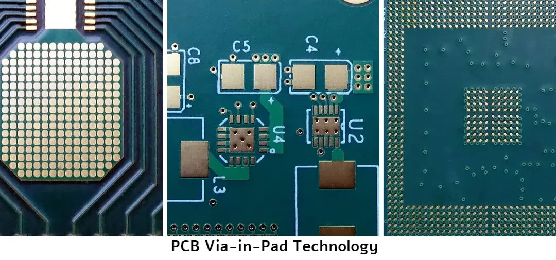
In solder mask design, it is essential to ensure appropriate expansion around pads to accommodate the selected solder surface finish. Lead-free finishes, which typically involve higher soldering temperatures, may require slightly greater expansion to cope with thermal stress. Precise alignment of the solder mask to the pad is critical, as misalignment can lead to solder bridging or poor solder joints. Regarding pad layout, maintaining consistent pad size and shape is vital for uniform solder joints. This is particularly important for lead-free soldering, where the harder and more brittle joints require precise pad design to prevent mechanical failure. Via-in-pad designs should be avoided unless properly filled and capped to prevent solder wicking and voiding.
Conclusion
The transition from lead to lead-free soldering in PCBA is driven by environmental and health considerations, presenting significant technical challenges. Understanding the differences in physical properties, process requirements, and potential failure modes is crucial for achieving reliable and high-quality solder joints in lead-free assemblies.
While lead-free soldering presents hurdles such as higher processing temperatures, increased oxidation, and potential reliability issues, these can be mitigated through careful process control, material selection, and design adaptation. As the industry continues to evolve, ongoing research and technological advancements will further enhance the reliability and performance of lead-free soldering in electronic manufacturing.

Recommended Posts
Comprehensive Analysis of PCB Via-in-Pad Technology
[pac_divi_table_of_contents...

PCB Hole Selection to Optimize PCB Performance and Cost
[pac_divi_table_of_contents...

PCB Manufacturing Process Flow – Ultimate Guide Is Here
[pac_divi_table_of_contents...

Exploring PCB Surface Treatment: The Significance of ENIG and DIG
PCB Surface Treatment:ENIG PCB With the ever-evolving...
Take a Quick Quote