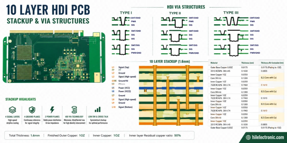
Figure 1. 10 layer HDI PCB engineering for microvias and BGA escape. Table of Contents When a 10 Layer Board Actually Needs HDI How to Read and Select 1+8+1, 2+6+2 and 3+4+3 Microvia Geometry, Capture Pads and Via-in-Pad Stacked, Staggered and Skip Microvias...