
The advantages and disadvantages of PCB surface finish

Printed Circuit Boards (PCBs) are the backbone of modern electronics, found in everything from smartphones to satellites. Their functionality and reliability heavily depend on the quality of the surface finish applied. This guide delves into the intricacies of PCB surface finishes, discussing their types, advantages, disadvantages, and the science behind their effectiveness.
Introduction to PCB Surface Finishes
Surface finishes are a critical aspect of printed circuit board (PCB) fabrication. They serve multiple functions:
- Protect the copper from oxidation and corrosion
- Provide good solderability for component attachments
- Ensure conductivity between joints
- Resist wear and abrasion during assembly and use
- Allow effective inspection and testing
This article explores the common PCB surface finish options in-depth, their advantages and limitations, and guidelines for selection.
Hot Air Solder Leveling (HASL)

HASL is the traditional approach for finishing PCBs, used since the 1960s. The steps include:
- Flux application to remove oxides and improve solder spread.
- Dipping boards in molten solder bath (typically tin-lead).
- Leveling the liquid solder using jets of hot air or nitrogen when withdrawn.
This leaves a coating of solder on the PCB pads and traces. Key process parameters are solder bath temperature, exposure time, air knife pressure and temperature.
HASL thickness ranges from 1-70 μm. The typical thickness is 20-30 μm. The dull HASL finish provides excellent solderability. The solder coating prevents oxidation and allows formation of reliable solder joints.
However, there are some disadvantages of HASL:
- Non-uniform thickness: The meniscus effect leads to uneven deposits.
- Limited shelf life: The finish eventually oxidizes over time.
- Not suitable for fine pitch: Risk of solder bridging on dense PCBs.
- Warping of thin boards: High temperatures can cause warpage.
- Flux residue trapping: Flux can get trapped under the solder.
- DFM challenges: HASL can create manufacturability issues.
Modifications like reducing the solder bath temperature help improve the process. Overall, HASL provides acceptable performance at low cost. But challenges exist for modern fine pitch designs.
Organic Solderability Preservatives (OSP)
OSP coatings are organic compounds applied on the PCB surface. They contain chemicals like imidazoles or benzimidazoles that react with copper oxide to form thin polymeric films.
The OSP layer thickness is 0.1-0.2 μm. The coatings act as a temporary protection against oxidation. But must also be removable during soldering to expose bare copper.
Advantages of OSP:
- Simple process by spraying or dipping
- Smooth finish comparable to ENIG
- Low cost and lead-free
- Suitable for fine pitch
Disadvantages:
- Limited shelf life
- Reworkability issues
- Difficult optical inspection
- Lower resistance to harsh environments
OSP is suitable for many consumer electronics applications. But higher reliability demands may need other finishes.
Immersion Silver and Immersion Tin
Immersion silver and tin are chemically deposited metal layers on PCBs by displacement reactions. PCBs are dipped in heated solutions with silver or tin ions. The ions replace copper atoms, plating the boards.
Typical thickness is 0.1-0.3 μm for immersion silver and 0.1-0.8 μm for immersion tin.
Advantages:
- Excellent solderability
- Lead-free and RoHS compliant
- Lower cost than gold finishes
- Simpler processing than electroless plating
Disadvantages:
- Tarnishing and oxidation over time
- Limited shelf life
- Whiskering risks with tin
- More rework needed with silver
These finishes suit many cost-sensitive consumer electronics. But stability concerns exist for long-life products.
Electroless Nickel Immersion Gold (ENIG)
ENIG involves initial electroless nickel plating followed by immersion deposition of a thin gold layer. The nickel coating is 3-6 μm thick while gold is 0.05-0.15 μm.
The nickel acts as a diffusion barrier layer and provides a good foundation for soldering. Gold offers superb corrosion resistance and conductivity.
Advantages of ENIG:
- Excellent shelf life
- Wear protection from gold layer
- Lead-free compatible
- Uniform and smooth finish
Disadvantages:
- High cost due to gold
- Tight process control needed
- Possible solderability loss over time
- Brittle deposits at thicknesses over 0.5 μm
ENIG is suitable for high-reliability and military-grade PCBs where cost is not a constraint.
Electrolytic Nickel/Gold (Hard Gold/Soft Gold)

Electrolytic nickel/gold refers to electroplated nickel and gold coatings on PCBs. There are two primary types:
Hard Gold
Hard gold has a higher nickel or cobalt content, resulting in lower purity of around 90-95%. It is harder and more wear-resistant.
Hard gold is commonly used for:
- Edge connectors and fingers – Withstands mating cycles
- Contact points – Handles switching arcs
- Connectors – Resists abrasion
Thickness can range from 2-10 μm based on wear requirements.
Soft Gold
Soft gold contains >99% pure gold. It offers maximum conductivity and corrosion resistance. Soft gold suits:
- Wire bonding – Enables high yield bonding
- Soldering – Provides excellent wettability
Typical thicknesses are 0.05-2 μm.
Advantages of Electrolytic Nickel/Gold
- Customizable thickness as needed
- Hard gold option for contacts/connectors
- Lead-free compatible
Disadvantages
- Very expensive, especially soft gold
- Lower initial solderability of hard gold
- Brittle at higher thicknesses
- Additional traces required for gold fingers
Electrolytic nickel/gold allows optimized performance but at higher cost.
Electroless Nickel Electroless Palladium Immersion Gold (ENEPIG)
ENEPIG enhances ENIG by adding an electroless palladium layer between the nickel and gold coatings. This further improves corrosion resistance.
The nickel layer thickness is ~3-6 μm. Palladium is ~0.1-0.5 μm while gold is 0.02-0.1 μm.
Advantages of ENEPIG
- Eliminates black pad risk with ENIG
- Better wire bondability than ENIG
- High corrosion and oxidation resistance
- Long shelf life
Disadvantages
- Very complex process control
- High cost due to multi-layer depositions
- Newer process, still maturing
- Often needs final flash gold plating
ENEPIG provides maximum protection for harsh environments. But is also the most expensive PCB finish.
Liquid Photoimageable Solder Masks (LPSIM)
LPSIM or Liquid Photoimageable Coatings (LPC) are UV-curable solder masks. They act as a permanent protective finish, eliminating the need for conformal coatings.
LPSIM is applied by screen printing or spraying. It is exposed and cured to form a tough protective polymeric layer.
Advantages of LPSIM:
- Excellent protection against environment/abrasion
- Improved process integration
- Higher resolution than dry film mask
- Withstands multiple reflows
Disadvantages:
- Limited post-application inspection
- Complex multiple processing steps
- Higher material and processing costs
- Thermal shock resistance concerns
Overall, LPSIM provides reliably high-performance protection. But at a higher cost than traditional solder masks.
Conclusion
The PCB surface finish has a substantial impact on manufacturability, soldering processes, inspectability, reliability and cost. Optimizing the finish requires evaluating key trade-offs based on the product’s life-cycle environment, quality targets and budget. This overview provides designers a comprehensive perspective on choosing the right finish for their application needs.

Recommended Posts
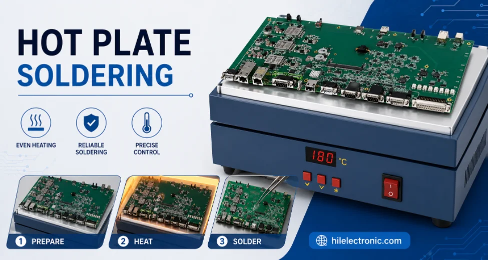
Hot Plate Soldering: Process, Limits, and Reflow Comparison
Figure 1. hot plate soldering image for Highleap...

Clean Flux vs No-Clean Flux: Residue, Cleaning, and PCB Reliability
Figure 1. clean flux vs no-clean flux image for Highleap...
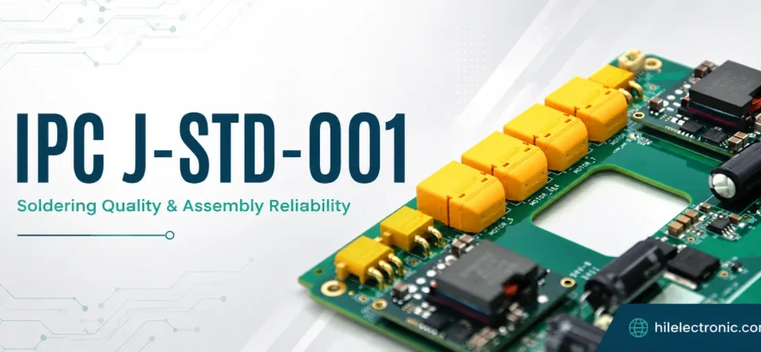
IPC J-STD-001: Classes, Requirements, and RFQ Specification
Figure 1. IPC J-STD-001 image for Highleap Electronics PCB...
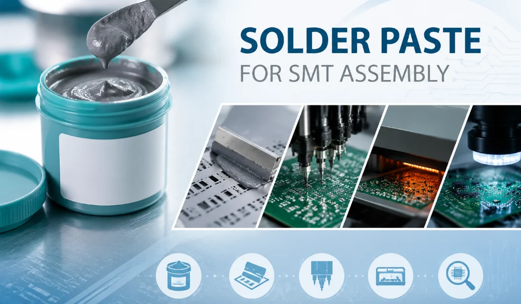
Solder Paste for SMT Assembly: Types, Storage, and Printing Defects
Figure 1. Solder paste selection affects SMT print...
Discover how our expertise can help with your next PCB project.