
PCB Essentials: Materials, Design, and Manufacturing Process

PCBs, or Printed Circuit Boards, are the backbone of modern electronics, powering everything from smartphones to satellites. Without them, today’s technology-driven world would come to a halt. At Highleap, we provide a one-stop solution for all your PCB needs, including PCB manufacturing, PCB assembly, PCB testing, and even PCB enclosures, ensuring your electronic designs are brought to life with precision and reliability. From prototypes to mass production, we tailor our services to meet the specific requirements of industries such as aerospace, automotive, medical, and consumer electronics.
In this guide, we’ll uncover the history, types, and advanced techniques involved in the PCB manufacturing process. You’ll learn how PCBs are designed, assembled, and tested to achieve high performance and reliability. Plus, we’ll highlight how Highleap’s expertise in areas like HDI PCBs with 2/2mil line spacing, flexible designs, and high-frequency applications ensures seamless integration into your projects, making us your trusted partner in innovation.
Definition and Purpose of PCBs
Printed Circuit Boards (PCBs) are the cornerstone of modern electronic devices, serving a critical role in the functionality and performance of a vast array of products. At their core, PCBs are mechanical structures meticulously engineered to support and electrically connect a multitude of electronic components in a highly organized and efficient manner.
The Role of PCBs in Modern Electronics
The primary purpose of a PCB is to replace the once cumbersome and error-prone wiring of early electronic systems. Before the advent of PCBs, connections were made with individual wires, leading to not only a tangle of connections but also increased size and reduced reliability of electronic devices. PCBs revolutionized this approach by providing a compact, reliable, and scalable solution.
Physical Platform for Electronic Components
A PCB acts as a physical platform, offering a base for mounting components such as resistors, capacitors, inductors, integrated circuits, and others. This platform is not just a passive substrate but an active part of the circuitry that includes a network of copper pathways etched onto non-conductive material, facilitating the transfer of electrical signals between components.
Facilitating Complex Connections
The intricate design of a PCB allows for complex circuits to be accommodated in a relatively small space. Through the use of multiple layers of conductive copper, separated by insulating materials, PCBs can house advanced circuits that are essential for the sophisticated functionalities demanded in today’s technology.
Enhancing Electrical Connectivity
The conductive copper tracks on a PCB are the lifelines of electronic circuits, providing a stable and durable path for electrical signals. These tracks are designed to adhere to specific widths and thicknesses to handle the required current and to minimize losses due to resistance, ensuring the device operates within its electrical specifications.
Supporting Advanced Technologies
As electronic devices have evolved to become more powerful and compact, PCBs have also advanced in design and materials. Multilayer PCBs, for instance, can consist of dozens of layers, accommodating the needs of high-speed and high-frequency circuits found in computers, smartphones, and other sophisticated electronics.
A Brief History of PCBS
The printed circuit board (PCB) is essential for the proper functioning of electronic devices. Throughout history, PCBs have evolved and taken on various roles to optimize electronics.
Initially, PCBs served as component holders, providing a platform for connecting electrical parts. Over time, they replaced the need for excessive wiring and cables. Today, PCBs have become the superstructure for high-speed designs, enabling efficient electronic performance.
The first PCB was developed in 1940 for proximity fuses used in artillery shells during World War II. This invention was groundbreaking as it allowed circuits to detect objects and explode when they approached. The success of this technology was significant for the UK during the war. Later, in 1947, the invention of the transistor revolutionized electronics and found its initial application in televisions.
In 1956, the US Army introduced the concept of etching copper boards, which revolutionized electronics manufacturing. This method involved etching desired traces on a plain copper surface, attaching components, and completing the board within 20 minutes. Although these early boards were one-sided, they represented a significant leap forward in electronics production.
Before PCBs became widespread, connecting components in appliances was a time-consuming and disorganized process. The integration of wires onto flat fiberglass made it possible to minimize complex electronic devices like smartphones and laptops.
Overall, the evolution of PCB technology has been remarkable. Today, PCBs play vital roles in enabling electronic devices, driving commerce, and facilitating information exchange. Their optimization and advancements have revolutionized the electronics industry, benefiting humanity in numerous ways.
Classification of PCB materials
PCB materials refer to the base materials used in printed circuit boards, which consist of copper foil and adhesive sheets. The most common and widely used PCB material is FR4, which is an epoxy or modified epoxy resin adhesive with glass fiber cloth as the reinforcing material. FR4 is a general name for this resin system, and it is extensively used in printed boards worldwide. The classification of PCB materials goes beyond FR4, and understanding the different resin systems is crucial for selecting the appropriate material for specific applications.Generally, FR4 is classified according to the following types:

- Glass Fiber Cloth Weaving
- Types: 106, 1067, 1080, 1078, 2116, 2113, 3313, 7628, etc.
- Defined in IPC specifications.
- Glass Type
- E-glass: Electrically insulating, calcium aluminosilicate, alkali-free.
- NE glass: Low dielectric fiber glass, lower dielectric constant and loss factor.
- Resin System and Properties by Supplier
- Lianmao Iteq: IT180A, IT170GRA1, IT958G, IT968, IT968SE, IT988GSE.
- Taiyao TUC: TU862HF, TU872LK, TU872SLK, TU872SLK-SP, TU883, TU933+.
- Panasonic: Megtron4, M4S, Megtron6, M6G, M7E, M7NE.
- Park Meteorwave Series: MW1000, 2000, 3000, 4000, 8000.
- Shengyi: S1000-2(M), S7439, S6, SH260, etc.
- Rogers: RO4003, RO3003, RO4350B, RT5880, RT5870, RO6006, RO3010 (RF material), etc.
- Isola: Isola 370HR, Isola FR408.
- Loss Level Classification
- Ordinary loss materials (DF ≥ 0.02).
- Medium loss materials (0.01 < DF < 0.02).
- Low loss materials (0.005 < DF < 0.01).
- Ultra-low loss materials (DF < 0.005).
- Flame Retardancy
- Flame retardant (UL94-VO, UL94-V1).
- Non-flame retardant (UL94-HB).
Types of PCBs (printed circuit boards)
There are several types of printed circuit boards (PCBs) available, each designed for specific applications and requirements. Here are some common types:
Single-sided PCB: This is the most basic type of PCB, with components mounted on one side and copper traces on the other. They are used in simple electronic devices with fewer components.
Double-sided PCB: These PCBs have components mounted on both sides, allowing for a higher density of components and more complex circuitry. Copper traces are present on both sides, and they are connected through vias or plated-through holes.
Multilayer PCB: Multilayer PCBs consist of multiple layers of copper traces separated by insulating layers (substrates). These layers are interconnected through vias, forming complex circuits. They are used in advanced electronic devices that require high-density circuitry and signal integrity.
Rigid PCB: Rigid PCBs are made from solid materials, such as fiberglass-reinforced epoxy, which provides rigidity and strength. They are commonly used in most electronic devices, from consumer electronics to industrial equipment.
Flexible PCB: Flexible PCBs, also known as flex PCBs, are made from flexible materials, such as polyimide. They can bend and conform to different shapes, making them suitable for applications that require flexibility, such as wearable devices, curved displays, and medical devices.
Rigid-Flex PCB: Rigid-flex PCBs combine the features of rigid and flexible PCBs. They consist of both rigid and flexible sections, allowing for complex designs and integration of multiple PCBs into a single unit. Rigid-flex PCBs are used in devices that require both flexibility and structural stability.
High-Frequency PCB: High-frequency PCBs are designed to handle high-frequency signals without significant signal loss or distortion. They use specialized materials and design techniques to minimize signal interference and maintain signal integrity. They are commonly used in communication systems, RF devices, and high-speed digital circuits.
High-Temperature PCB: High-temperature PCBs are designed to withstand elevated temperatures without degradation. They use materials with high glass transition temperatures and specialized solder masks and laminates to withstand the heat generated by components or harsh environments.
HDI PCB: HDI PCB (High-Density Interconnect PCB) are designed to maximize the density of components and interconnections. They utilize advanced manufacturing techniques such as microvias, blind vias, and buried vias to achieve high-density circuitry. HDI PCBs are commonly used in compact electronic devices like smartphones, tablets, and medical equipment.
Metal Core PCB : Metal core PCBs(MCPCB) have a metal substrate, typically aluminum or copper, that provides excellent heat dissipation capabilities. They are commonly used in applications that require efficient heat management, such as LED lighting, power electronics, and automotive applications.
Ceramic PCB: Ceramic PCBs use a ceramic substrate instead of traditional epoxy or fiberglass materials. Ceramic offers excellent thermal conductivity, high electrical insulation, and stability at high temperatures. These PCBs are commonly used in high-power electronic applications, RF devices, and aerospace applications.
PCB Design and Manufacturing Process
The PCB design and manufacturing process is a complex and highly organized sequence of steps that involves converting a circuit schematic into a physical, functional printed circuit board (PCB). This process ensures that electronic components are properly connected and mounted on the PCB, resulting in a reliable and efficient electronic device. Here is a detailed overview of the PCB design and manufacturing process:
1. Conceptualization and Design Requirements
- Project Definition: The process begins with a clear understanding of the project requirements and objectives. Designers must determine the PCB’s purpose, functionality, and specific technical specifications.
2. Schematic Design
- Schematic Capture: Designers create an electrical schematic diagram using specialized PCB design software. This diagram represents the logical connections between electronic components and their functions.
3. Component Selection and Placement
- Component Library: Designers select electronic components from a component library provided by the PCB design software. This library contains detailed information about each component, including electrical characteristics, footprints, and 3D models.
- Component Placement: Components are placed on the PCB layout according to the schematic diagram. Considerations include component orientation, spacing, and thermal management.
4. PCB Layout
- Routing: Designers use the PCB design software to route electrical traces (copper conductors) between components based on the schematic. The routing must adhere to design rules and constraints, considering factors like signal integrity, impedance matching, and power distribution.
- Layer Stackup: The layer stackup, specifying the arrangement of conductive and insulating layers, is determined based on the PCB’s complexity and requirements.
- Signal Ground Planes: Ground planes are created to ensure proper grounding and minimize electromagnetic interference (EMI).
- Signal Traces: Critical signal traces may require controlled impedance, differential pairs, or other specific routing techniques.
- Power Planes: Adequate power distribution and management are essential to provide a stable supply voltage to components.
5. Design Verification
- Design Rule Check (DRC): The PCB design software performs automated checks to ensure that the layout adheres to design rules, such as minimum trace spacing, minimum drill size, and clearance requirements.
- Electrical Simulation: Some designs may require electrical simulations to verify signal integrity and performance.
6. Gerber File Generation
- Gerber Files: The PCB layout is converted into Gerber files, which contain detailed information about the PCB’s physical layers, including copper traces, drill holes, and solder mask.
7. Prototype Fabrication
- Ordering PCBs: Gerber files are sent to a PCB manufacturer for fabrication. The manufacturer produces prototype PCBs according to the design specifications.The picture below is the conventional board production process flow chart of Highleap factory.

8. Assembly
- Component Placement: Electronic components are mounted onto the fabricated PCB using either manual or automated assembly processes.
- Soldering: Components are soldered to the PCB using techniques like reflow soldering or wave soldering.
9. Testing and Quality Control
- Functional Testing: The assembled PCBs undergo functional testing to ensure they operate as intended.
- Quality Control: Inspection and quality control processes are carried out to identify and rectify any defects or issues.
10. Final Product Integration
- Integration into Devices: The PCBs are integrated into the final electronic devices or systems.
Throughout the PCB design and manufacturing process, collaboration between designers and manufacturers is crucial to ensure that the final PCB meets both electrical and mechanical requirements. Advanced design software and manufacturing techniques have greatly enhanced the efficiency and precision of this process, enabling the production of highly complex and reliable PCBs for a wide range of applications in the electronics industry.
PCB Main Functions and Characteristics
PCB(Printed Circuit Board), or Printed Circuit Boards, serve as the backbone for virtually all modern electronic devices. Here’s a summary of their key functions and characteristics:
- Electrical Connectivity: PCBs are essentially the conduits for electricity in electronic devices. They create the necessary connections between various electronic components, ensuring that electrical signals can flow where they are needed to make circuits work as designed.
- Mechanical Support: Beyond just electrical pathways, PCBs provide physical support to electronic components. They serve as a sturdy base that keeps all the components securely in place, which is vital for the overall durability and function of the device.
- Signal Integrity: PCBs are designed to preserve the integrity of the signals that pass through them. This is achieved by controlling the impedance, minimizing noise and interference, and managing the layout of signal paths. Good signal integrity is crucial for the device to function accurately and reliably.
- Heat Management: The components on a PCB can generate a lot of heat during operation. PCBs help manage this heat through various means, like thermal vias and heatsinks, ensuring that components don’t overheat and the device operates within safe temperature limits.
- Size Optimization: Space is often at a premium in electronic devices, especially portable ones. PCBs allow for the dense packing of components, enabling the creation of compact devices without sacrificing functionality.
- Maintenance and Repair: The way PCBs are designed often allows for easier maintenance and repair. If a component fails, it can often be replaced without the need to discard the entire board, making the device more serviceable.
- Reliability and Stability: A well-designed and well-made PCB can be incredibly reliable, maintaining its performance over time despite environmental stresses like temperature changes and physical shocks or vibrations.
In essence, PCBs are critical for the operation of modern electronics, providing the necessary infrastructure for electrical functionality, physical stability, and long-term reliability of devices.
PCB Design and Manufacturing Software Tools
PCB design and manufacturing rely on a variety of specialized software tools to transition from concept to final product. Below are examples for both categories.
PCB Design Software Features
- EAGLE
- Schematic editor for creating circuit diagrams.
- PCB layout editor for designing PCB layouts.
- Library content with thousands of component footprints and symbols.
- User Language Programs (ULPs) for customization and feature enhancement.
- KiCad
- Cross-platform and open-source with an integrated environment.
- Schematic capture and PCB layout with 3D viewer.
- No limit on the size of the PCB or the number of layers and components.
- Large user community and extensive libraries.
- Altium Designer
- Unified design environment for schematic and PCB design.
- Advanced routing technologies, including differential pair routing and trace length matching.
- Real-time cost estimation and tracking.
- Integration with Altium 365 cloud platform for collaboration and version control.
- OrCAD / Cadence Allegro
- Comprehensive suite for schematic capture, circuit simulation, and PCB design.
- High-speed design capabilities with constraint-driven design.
- Real-time interactive 3D canvas for PCB design.
- Advanced layout and miniaturization features.
- Mentor Graphics PADS
- Advanced PCB design solutions tailored for engineers and makers.
- Simulation and analysis with thermal and vibration analysis.
- Constraint management for ensuring design intent is maintained.
- Centralized library and part management.
- Proteus
- Integrated suite with schematic capture, PCB design, and simulation.
- Microcontroller simulation for virtual prototyping.
- Advanced routing and editing tools.
- Extensive component libraries.
- DipTrace
- Intuitive user interface with multi-sheet and multi-level hierarchical schematics.
- Smart manual routing tools and automatic router.
- 3D PCB Preview and export for mechanical CAD modeling.
- Thousands of library components and patterns.
- DesignSpark PCB
- No limitations on the design size or complexity.
- Schematic capture and PCB layout with a straightforward interface.
- Online component and model libraries.
- Integration with RS Components’ and Allied Electronics’ databases for parts selection.
- SolidWorks PCB
- Collaboration between electrical and mechanical design teams.
- Schematic capture and PCB layout integrated with SolidWorks CAD.
- Real-time 3D clearance checking.
- ECAD/MCAD project collaboration server for design collaboration.
Auxiliary Software for PCB Manufacturing Features
- CAM350
- Streamlines the transition from design to production.
- Design for Manufacture (DFM) analysis to reduce cycle time and improve yield.
- Detailed reporting on design and layer stackup information.
- Genesis2000
- Advanced CAM and engineering solutions for PCB manufacturing.
- Automation tools for reducing pre-production time.
- Quality control features, including etch compensation and solder mask generation.
- InCAM
- Advanced CAM software for high-level engineering of PCBs.
- Capabilities for editing, process engineering, and verification.
- Automation of complex CAM tasks and detailed DFM checks.
- Valor MSS
- End-to-end solution for PCB assembly and manufacturing.
- Product modeling and simulation for assembly and test processes.
- Integration with ERP/MRP systems for materials and process management.
- BluePrint-PCB
- Automated creation of comprehensive electronic drawings.
- Integration with CAM350 for design and manufacturing preparation.
- Facilitates communication and collaboration between PCB design and manufacturing.
- UCAMCO UcamX
- High-precision CAM tool for front-end engineering in PCB manufacturing.
- Extensive automation capabilities to reduce manual input.
- Full data integrity check to ensure manufacturability.
- Fabmaster
- Specifically tailored for the PCB assembly process.
- Supports a variety of file formats for PCB data import.
- Tools for optimizing production flow and enhancing machine programming.
These software tools are selected based on their strengths in handling the various aspects of PCB design and manufacturing, such as ease of use, advanced capabilities, industry compliance, and the ability to manage complexity.
Conclusion
PCBs are an essential part of our daily lives, quietly powering the devices and systems we rely on. From the simplest single-layer boards to advanced HDI and flexible PCBs, they enable the functionality, efficiency, and innovation behind modern technology. Whether it’s ensuring signal integrity in high-speed applications or managing heat in power electronics, PCBs are at the heart of it all.
At Highleap, we understand the critical role PCBs play in your projects. That’s why we offer end-to-end solutions, from manufacturing and assembly to testing and custom enclosures, tailored to meet the needs of industries like telecommunications, medical devices, automotive, and consumer electronics. With precision engineering and a commitment to quality, we’re here to help you turn your concepts into reality. Contact us today to see how we can support your next big idea with reliable and high-performance PCBs.
FAQ
1. What is the minimum trace width and spacing achievable in PCB manufacturing?
We can achieve a minimum trace width and spacing of 2/2mil, perfect for high-density designs such as HDI PCBs, ensuring compact layouts without compromising performance.
2. What materials are commonly used in PCB manufacturing?
The most common materials include FR4 for general applications, Rogers and Teflon for high-frequency PCBs, and polyimide for flexible PCBs. Material choice depends on factors like heat resistance, dielectric properties, and signal performance.
3. How do you ensure signal integrity in high-speed PCB designs?
Signal integrity is maintained through controlled impedance, differential pair routing, proper layer stackups, and reducing crosstalk by carefully spacing traces. For RF and high-speed designs, materials like Rogers are used to minimize signal loss.
4. What is the difference between single-layer, double-layer, and multilayer PCBs?
- Single-layer PCBs: Have components and copper traces on one side, suitable for simple designs.
- Double-layer PCBs: Have copper traces on both sides, allowing more complex circuits.
- Multilayer PCBs: Contain multiple layers of copper separated by insulating material, ideal for advanced designs requiring high-density circuits.
5. What is an HDI PCB, and why is it used?
HDI (High-Density Interconnect) PCBs feature finer lines, smaller vias (microvias), and more interconnections per unit area. They are commonly used in compact devices like smartphones and wearables, where space optimization and performance are crucial.
6. How are flexible PCBs different from rigid PCBs?
Flexible PCBs are made with materials like polyimide, allowing them to bend and fold, which is ideal for applications like medical devices and wearables. Rigid PCBs, made from materials like FR4, offer structural stability and are used in most electronic devices.
7. What is the purpose of solder masks on PCBs?
Solder masks protect the copper traces from oxidation, prevent solder bridges during assembly, and add durability to the PCB. They also enhance the appearance of the board with their distinctive colors.
8. How is heat managed in PCBs?
Heat is managed using thermal vias, heatsinks, metal-core PCBs, and proper component placement. High-power applications often use aluminum or copper-core PCBs to dissipate heat effectively.
9. What are the testing methods used in PCB manufacturing?
Common testing methods include:
- Flying probe testing: For continuity and shorts.
- Automated Optical Inspection (AOI): To detect visual defects.
- X-ray inspection: For checking internal layers and solder joints.
- Impedance testing: For high-speed designs to ensure signal quality.
10. What are via types in PCB designs, and when are they used?
- Through-hole vias: Connect all layers of a PCB.
- Blind vias: Connect an outer layer to an inner layer.
- Buried vias: Connect internal layers only.
- Microvias: Extremely small vias used in HDI PCBs for compact designs.
11. What is impedance control in PCBs, and why is it important?
Impedance control ensures consistent signal transmission in high-frequency circuits. It involves designing trace widths, spacing, and layer stackups to match specific impedance values, preventing signal loss and distortion.
12. How do you choose the right PCB material for high-frequency designs?
High-frequency designs require materials with low dielectric loss and high thermal stability. Rogers, Teflon, and ceramic-based materials are commonly used to maintain signal integrity and minimize interference.
13. What finishes are available for PCBs, and how do they differ?
- ENIG (Electroless Nickel Immersion Gold): Long shelf life, great for solderability.
- HASL (Hot Air Solder Leveling): Cost-effective but less precise.
- OSP (Organic Solderability Preservative): Low-cost, suitable for short-term use.
- Immersion Silver/Tin: Suitable for high-speed and press-fit applications.
14. What is the difference between rigid-flex PCBs and multilayer PCBs?
Rigid-flex PCBs combine rigid and flexible sections, making them ideal for applications where both stability and flexibility are required (e.g., aerospace and medical). Multilayer PCBs, on the other hand, are entirely rigid and designed to support complex circuits in a stable format.
15. What factors affect PCB manufacturing lead time?
Lead time depends on:
- PCB complexity (e.g., layer count, HDI features).
- Material availability (e.g., specialized materials like Rogers).
- Testing and quality control requirements.
Prototypes can be completed in 5–7 days, while production orders may take 2–3 weeks depending on these factors.

Recommended Posts
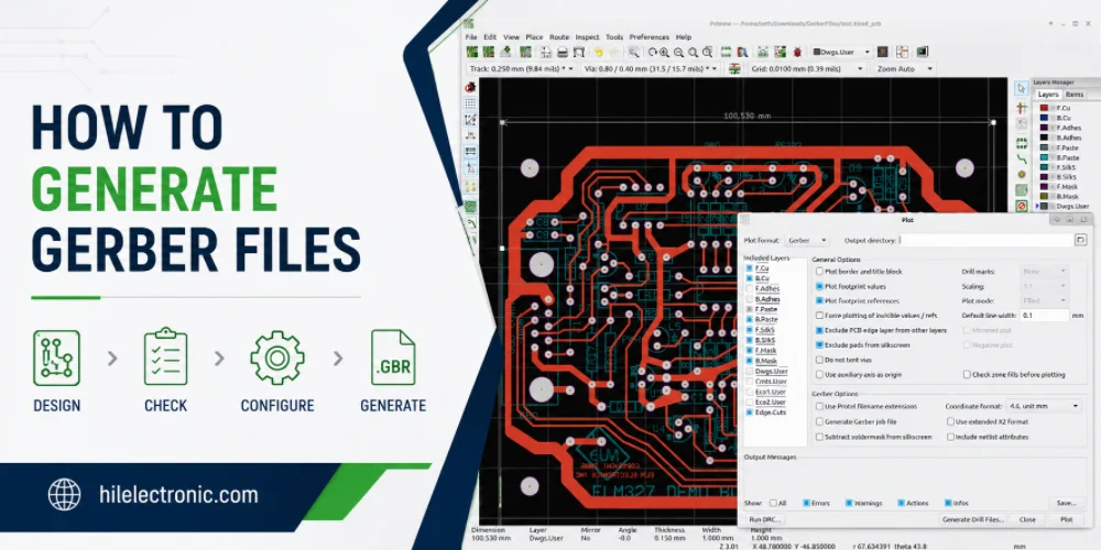
How to Generate Gerber Files for PCB Manufacturing
Figure 1. how to generate Gerber files image for Highleap...
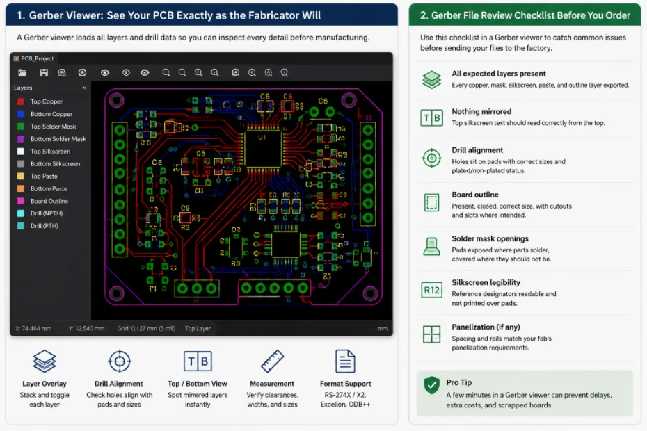
Gerber File Review Checklist: How to Check PCB Files Before You Order
Figure 1. Gerber file review catches missing layers, drill...
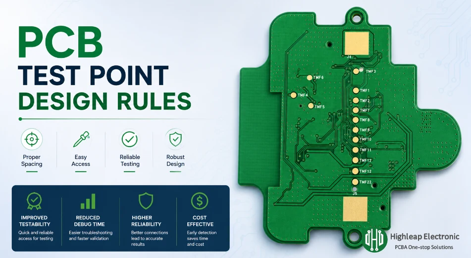
PCB Test Point Design Rules for Debug and ICT
Figure 1. PCB test point design rules help make debugging,...
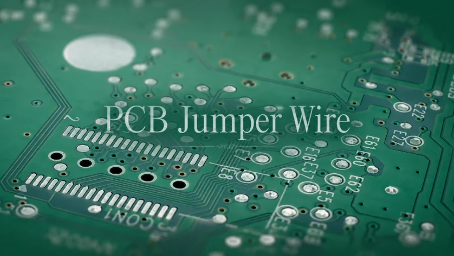
PCB Jumper Wire: Uses, Types, and Design Tips
Figure 1. PCB jumper wires are useful for prototypes and...
How to get a quote for PCBs
Let us run DFM/DFA analysis for you and get back to you with a report.
You can upload your files securely through our website.
We require the following information in order to give you a quote:
-
- Gerber, ODB++, or .pcb, spec.
- BOM list if you require assembly
- Quantity
- Turn time
In addition to PCB manufacturing, we offer a comprehensive range of electronic services, including PCB design, PCBA (Printed Circuit Board Assembly), and turnkey solutions. Whether you need help with prototyping, design verification, component sourcing, or mass production, we provide end-to-end support to ensure your project’s success. For PCBA services, please provide your BOM (Bill of Materials) and any specific assembly instructions. We also offer DFM/DFA analysis to optimize your designs for manufacturability and assembly, ensuring a smooth production process.