
Single Layer PCB (Single Sided PCB) Made in China

Single Layer PCBs, or Single-Sided PCBs, are fundamental components in electronics, consisting of only one conductive layer and a single mounting side for components. Their simplicity and affordability make them ideal for various low-density applications, offering a practical and cost-effective solution for electronic devices ranging from calculators to LED systems. Despite the advent of multi-layer PCBs, single-layer designs remain popular in specific applications due to their ease of design, reduced cost, and straightforward manufacturing process.
What is a Single Layer PCB?
A Single Layer PCB, also known as a Single-Sided PCB, includes one conductive layer (usually copper) on a single side of a non-conductive substrate. The single conductive layer carries electrical signals, while the other side of the board is used to mount components. Unlike double-sided or multi-layer boards, single-layer PCBs are less complex but sufficient for straightforward electronic circuits and applications where intricate circuitry isn’t required.
The simplicity of a single-layer PCB makes it an ideal choice for designers aiming to keep costs low and minimize production complexities, especially for projects that do not demand high-speed signal processing or extensive functionality.
Types of Single Layer PCBs
Single layer PCBs are versatile and can be categorized into different types based on their material and application. Here’s a breakdown of common single-sided PCB variations:
- Rigid Single Layer PCB: Built on rigid materials like FR-4 (fiberglass epoxy), these boards are inflexible, offering structural stability and durability. Commonly used in products like power supplies and home appliances, rigid single-layer PCBs provide a solid foundation for components.
- Flexible Single Layer PCB: Flexible PCBs use bendable materials, such as polyimide, which makes them suitable for devices requiring flexibility, like wearable electronics. Although more costly to produce than rigid single-layer PCBs, flexible PCBs offer design versatility by fitting into compact spaces or curved surfaces.
- Rigid-Flex Single Layer PCB: Combining the strengths of rigid and flexible PCBs, these designs are beneficial in applications that require both structural stability and flexibility, such as medical devices and complex industrial equipment.
- High-Frequency Single Layer PCB: These are built using specialized materials (e.g., Rogers, Taconic) to manage high-frequency signal processing, making them ideal for RF applications where signal integrity is critical.
- Aluminum Single Layer PCB: In these boards, an aluminum substrate replaces the traditional FR-4 base. Aluminum single-layer PCBs are favored for applications needing high heat dissipation, such as LED lighting systems, as the aluminum substrate provides excellent thermal conductivity.
Key Benefits of Single Layer PCBs
Single layer PCBs have several advantages, especially for simpler and cost-sensitive applications. Below are some of the key benefits of using single-sided PCBs:
- Cost-Effective Production: The design simplicity of single-layer PCBs requires fewer resources and processes, resulting in lower production costs. This makes single-layer PCBs ideal for high-volume production and budget-conscious projects.
- Ease of Design and Manufacturing: With a single layer to design and manufacture, single-sided PCBs are easier to produce, leading to quicker turnaround times and simpler production. This efficiency is ideal for prototyping and rapid production cycles.
- Reliability and Durability: Due to their uncomplicated structure, single-sided PCBs are generally more reliable, with fewer points of failure. They are easier to inspect, test, and repair, which increases their overall durability and reduces maintenance costs.
- Optimized for Low-Density Designs: For devices that do not require complex circuitry, such as LED lights or basic power supplies, single-layer PCBs provide ample space and performance without the need for additional layers.
- Efficient Heat Dissipation: In cases where aluminum substrates are used, single-layer PCBs offer improved heat dissipation, enhancing performance in applications with high thermal demands.
Applications of Single Layer PCBs
Single-layer PCBs are well-suited to applications where simple circuitry is adequate and cost control is a priority. Some typical applications include:
- Consumer Electronics: Single-layer PCBs are found in everyday consumer devices like calculators, remote controls, and digital clocks.
- Lighting Systems: These boards are ideal for LED lighting systems, which require straightforward circuit designs with efficient heat dissipation, often achieved using aluminum substrates.
- Household Appliances: Many home appliances, such as washing machines, coffee makers, and refrigerators, incorporate single-layer PCBs for basic control functions.
- Power Supplies: Single-layer PCBs are used in low-power AC-DC and DC-DC power supplies, where simple circuit structures suffice.
- Automotive Systems: Basic automotive electronics, such as lighting modules and power window controllers, benefit from the affordability and reliability of single-sided PCB designs.
- Industrial Equipment: Simple industrial controllers and sensors use single-layer PCBs for efficient and durable performance in routine, non-critical functions.
Single Layer PCB Manufacturing Process
Manufacturing a single layer PCB, also known as a single-sided PCB, involves multiple precise and carefully sequenced stages. This process ensures that each PCB meets strict specifications for quality, functionality, and durability. Below is the accurate manufacturing process for single layer PCBs, from design file preparation to final testing.
Step 1: Order Placement and Design for Manufacturing (DFM) Check
The manufacturing process begins when the order is placed and the PCB design files are received. Design engineers typically use PCB software such as Altium, Eagle, or KiCad to create the layout, which is then exported in Gerber format. Gerber files contain essential information, including copper layer patterns, drill files, solder masks, and silkscreen details.
Upon receiving the design, the manufacturer conducts a Design for Manufacturing (DFM) check. This check evaluates the design against manufacturing tolerances, ensuring that details like trace width, spacing, and hole sizes align with production capabilities. DFM ensures efficient production and minimizes errors or delays.
Step 2: PCB Board Cleaning and Cutting
Once the design passes the DFM check, the raw PCB material, usually FR-4 (fiberglass epoxy) or aluminum for heat-sensitive applications, is cut to the required dimensions. This base material will eventually form the structure of the PCB, with copper laminated on one side.
Before proceeding, the board undergoes a thorough cleaning to remove any dust or contaminants that could interfere with adhesion or subsequent processing. Cleanliness at this stage is critical to achieving reliable and consistent circuit patterns.
Step 3: Drilling and Hole Preparation
In this stage, holes are drilled into the PCB to create spaces for through-hole components or mounting points. High-precision CNC machines drill these holes according to specifications provided in the Gerber file.
The accuracy of the drilling process is essential, as improper hole alignment or size could affect component placement and overall board functionality. After drilling, the board is cleaned again to remove any dust or debris left by the drilling process.
Step 4: Electroplating
Electroplating prepares the board for copper plating, which is crucial for reliable electrical connections. This process involves placing the drilled PCB into a series of chemical baths that deposit a thin layer of copper across the surface and inside the drilled holes.
The copper layer formed in this step creates the foundation for circuit paths and enables connections for through-hole components. Proper electroplating is vital to ensure that the board conducts electricity effectively.
Step 5: Copper Plating
After electroplating, an additional copper layer is applied to the PCB to form the conductive circuits. This copper layer will eventually form the traces, pads, and other conductive elements of the PCB. The copper plating is applied uniformly to ensure consistent conductivity throughout the board.
The thickness of this copper layer is controlled according to design requirements, as it impacts the board’s electrical characteristics and thermal management.
Step 6: Circuit Pattern Printing
To create the specific circuit design, a photo-sensitive material called photoresist is applied to the copper-plated surface. A film with the circuit pattern, derived from the Gerber file, is aligned over the board, and the setup is exposed to UV light.
The UV exposure hardens the areas of photoresist that should remain as part of the circuit, while the unexposed areas remain soft. This stage transfers the circuit pattern precisely onto the PCB.
Step 7: Etching
In the etching process, the board is submerged in a chemical solution that removes the unprotected copper, leaving only the copper traces covered by hardened photoresist. This etching process defines the circuit paths and creates the conductive traces on the board.
After etching, the hardened photoresist is removed, leaving the desired copper circuitry intact. This step is essential to establish the electrical pathways needed for the circuit design.
Step 8: Automated Optical Inspection (AOI)
After the etching process, the board undergoes an Automated Optical Inspection (AOI). AOI uses high-resolution cameras to capture images of the board, comparing them against the original design to identify any defects or inconsistencies.
AOI helps ensure that the etched pattern accurately matches the design and that there are no open circuits, shorts, or other flaws in the circuit traces.
Step 9: Solder Mask Application
Once the circuit pattern is confirmed, a solder mask is applied to the PCB. The solder mask is a protective layer that covers the board’s surface, insulating the copper traces and preventing accidental shorts during assembly. The solder mask also protects the board from environmental factors, such as moisture and contaminants.
A film with the solder mask pattern is aligned over the PCB, and UV light is used to harden the exposed areas. The unhardened portions are then washed away, leaving the solder mask only on specified areas.
Step 10: Silkscreen Application
The silkscreen layer is added to print labels, component identifiers, and other markings on the PCB surface. This layer assists in assembly and testing by providing clear visual guidance on component placement and identification.
The silkscreen is typically printed using an inkjet printer or screen printing, depending on the design requirements. White is the most common color for silkscreen, but other colors can be used.
Step 11: Surface Finish Application
To enhance solderability and protect exposed copper pads, a surface finish is applied. Common finishes include HASL (Hot Air Solder Leveling), ENIG (Electroless Nickel Immersion Gold), or silver plating. The surface finish provides a protective layer that prevents oxidation and ensures durable, high-quality solder joints.
The type of finish is selected based on the application, budget, and desired longevity of the PCB.
Step 12: Electrical Testing (Flying Probe Test)
Electrical testing verifies the functionality and integrity of the PCB. In single-layer PCBs, a flying probe test is often used. This test employs movable probes that contact specific points on the board to measure connectivity, continuity, and detect any short circuits or open circuits.
This quality control step is essential to ensure that the board meets all electrical specifications before moving to assembly.
Step 13: Final Profiling and V-Scoring
The final step in the single layer PCB manufacturing process involves cutting the board to its specified dimensions. Profiling can be performed using either a router or a V-groove cutter. Routing leaves small tabs around the edges, while V-scoring creates grooves that allow the board to snap out from the production panel.
This final step completes the manufacturing process, resulting in individual PCBs that are now ready for assembly or further processing as required by the application.
Selecting the Optimal Base Material for Single Sided PCBs
Choosing the right base material for a Single Sided PCB (Single Layer PCB) is essential to ensure that the board performs effectively and meets the demands of its application. The base material impacts not only durability and performance but also thermal management and flexibility. Below are some of the most commonly used materials, each suited to specific application needs:
-
FR-4: FR-4 is a durable, fiberglass-reinforced epoxy that balances cost-effectiveness with stability, making it ideal for a wide range of standard electronic applications. Known for its insulation properties and moisture resistance, FR-4 is used in household electronics, consumer devices, and general-purpose products.
-
Aluminum: Aluminum substrates are preferred in applications where thermal management is critical, such as LED lighting, power supplies, and automotive electronics. Aluminum’s high heat dissipation capabilities prevent overheating and improve the lifespan of components in high-power setups.
-
Polyimide: Polyimide is known for its flexibility and resilience, making it an excellent choice for applications that demand bending or flexibility, like wearable technology and compact devices. It withstands high temperatures and environmental stress, ensuring reliability in applications where the board may be subjected to motion or extreme conditions.
-
Teflon (PTFE): For high-frequency and RF applications, Teflon (PTFE) is favored due to its low dielectric loss and stable electrical properties. It maintains signal clarity and integrity, which is crucial in telecommunications and other high-frequency applications where accurate signal transmission is paramount.
Selecting the appropriate base material for a Single Sided PCB ensures that the board meets the performance and environmental requirements of the application. The material affects everything from thermal handling to flexibility and signal quality, so it’s crucial to align material choice with the specific operational demands of the device.

Aluminum PCB Type
Key Factors Influencing the Cost of Single Sided PCBs
The cost of producing a Single Sided PCB (Single Layer PCB) is influenced by several key factors, starting with material selection. Different materials, such as FR-4, aluminum, polyimide, or Teflon (PTFE), each offer specific benefits in terms of durability, flexibility, and thermal management, but these features come at varying price points. For instance, aluminum substrates provide excellent heat dissipation, making them ideal for high-power applications like LED lighting, though they cost more than standard FR-4. Likewise, materials like polyimide and PTFE are ideal for flexible or high-frequency applications, but their added capabilities reflect a higher base cost. Selecting the appropriate material for the intended application is a foundational cost consideration.
Board size and circuit complexity also play a significant role in determining the cost of a Single Sided PCB. Larger boards require more raw materials, and intricate circuit designs involve tighter tolerances, precise routing, and sometimes additional layers for protective coatings, each of which adds to production time and expense. Additional factors include the choice of surface finish (such as ENIG or HASL) and copper thickness, both of which influence durability, electrical performance, and cost. Furthermore, testing and quality control requirements, like Automated Optical Inspection (AOI) or advanced functional testing, add to the production cost but ensure reliability, especially important in applications such as automotive or medical devices where performance is critical.
Lastly, order volume and lead time directly affect the per-unit cost of single-sided PCBs. High-volume orders benefit from economies of scale, reducing the per-unit price due to the efficiencies gained from bulk production and material procurement. Conversely, low-volume or prototype orders tend to have higher per-unit costs because setup and tooling fees remain the same regardless of quantity. Additionally, expedited lead times require manufacturers to allocate more resources or prioritize production, which can further increase costs. Understanding these factors allows for strategic planning in terms of both budget and project requirements, enabling manufacturers to optimize cost without compromising on quality.
Conclusion
Single layer PCBs remain a crucial component in electronics, offering simplicity, cost-efficiency, and reliability. Their manufacturing process, while less complex than multi-layer PCBs, requires precision and attention to detail to ensure quality and performance. By choosing the right materials, understanding the manufacturing process, and optimizing design for cost, single-sided PCBs continue to serve a wide range of applications from consumer electronics to industrial systems.
For manufacturers and designers, partnering with an experienced PCB provider ensures high-quality production, enabling effective product development and reliable performance in real-world applications.
FAQ for Single Sided PCB Costs and Production
- What materials are best suited for single sided PCB applications?
Single sided PCBs commonly use materials like FR-4 for general electronics, aluminum for high thermal conductivity in power-intensive applications, and polyimide for flexible designs. The choice depends on factors such as heat dissipation needs, flexibility, and the specific environmental requirements of the application. - How does the choice of surface finish impact the cost and durability of single sided PCBs?
Surface finishes such as HASL are cost-effective and suitable for many standard applications, while ENIG and silver finishes, though more costly, offer enhanced durability and corrosion resistance. The specific surface finish selected impacts both the lifespan of the PCB and the production cost. - What is the role of testing in single sided PCB production costs?
Testing options like AOI or functional testing add to production costs but are crucial for ensuring PCB quality, especially in high-reliability fields such as automotive and medical devices. These tests help detect potential defects early, ensuring that the final product meets the necessary standards. - Does bulk ordering significantly lower the cost per unit for single sided PCBs?
Yes, ordering in bulk reduces the cost per unit due to economies of scale, as setup, tooling, and material costs are distributed across a larger quantity. Bulk orders allow manufacturers to optimize production efficiency, making single sided PCBs more economical for high-volume needs. - How does board complexity affect the overall production cost of single sided PCBs?
The complexity of the circuit design and board layout increases production costs, as intricate patterns require precise routing, higher accuracy in drilling, and additional inspection steps. Simplified designs help control costs, but complex layouts may be essential for applications with specific functionality or space constraints.
Get a Free PCB & PCBA Quote

Recommended Posts
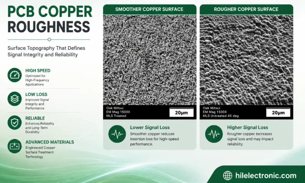
PCB Copper Roughness: Signal Loss, Material Selection and Manufacturing Control
Table of contentsWhat Is PCB Copper Roughness?How Copper...
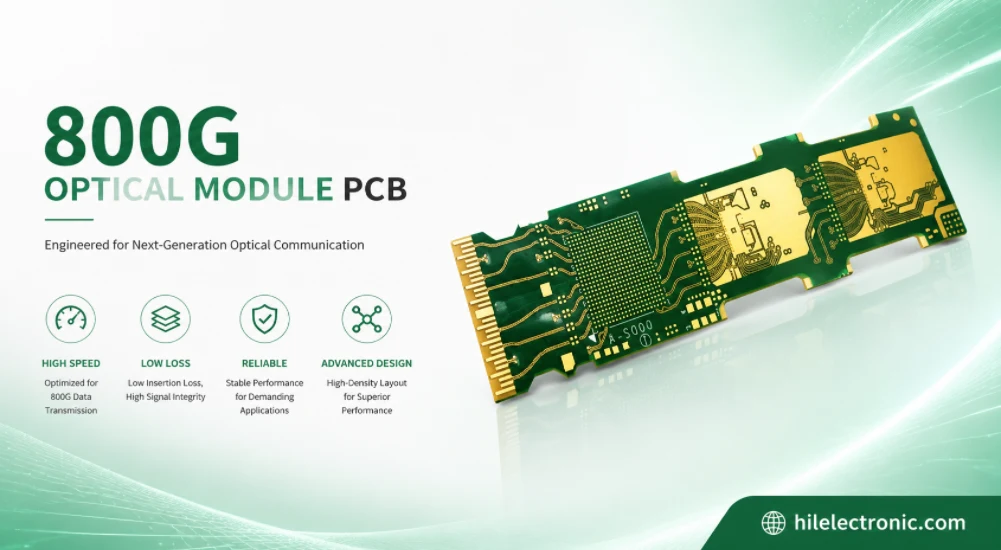
800G Optical Module PCB Manufacturing and Assembly Service
Table of contentsWhat Makes an 800G Optical Module PCB...
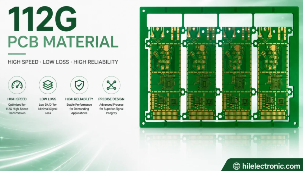
112G PCB Material Selection and High-Speed PCB Manufacturing
Table of contentsWhat “112G PCB Material” Actually...
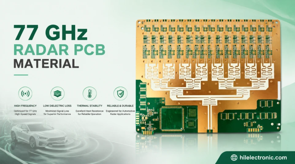
77 GHz Radar PCB Material Selection and Manufacturing Guide
Table of contentsWhat 77 GHz Changes in a PCBCommon 77 GHz...
How to get a quote for PCBs
Let us run DFM/DFA analysis for you and get back to you with a report.
You can upload your files securely through our website.
We require the following information in order to give you a quote:
-
- Gerber, ODB++, or .pcb, spec.
- BOM list if you require assembly
- Quantity
- Turn time
In addition to PCB manufacturing, we offer a comprehensive range of electronic services, including PCB design, PCBA (Printed Circuit Board Assembly), and turnkey solutions. Whether you need help with prototyping, design verification, component sourcing, or mass production, we provide end-to-end support to ensure your project’s success. For PCBA services, please provide your BOM (Bill of Materials) and any specific assembly instructions. We also offer DFM/DFA analysis to optimize your designs for manufacturability and assembly, ensuring a smooth production process.