
PCB Board Design: Essential Calculations, Principles, and Manufacturing Expertise

PCB board design is the backbone of modern electronics, providing the foundation for devices ranging from smartphones to aerospace systems. Effective PCB design isn’t just about placing components; it requires precise calculations to ensure signal integrity, thermal management, and power efficiency, particularly in high-speed and high-power applications. By mastering essential design principles and formulas for trace width, impedance, and voltage stability, engineers can create reliable, high-performance circuits suited to the complex needs of today’s industries. At Highleap Electronic, we specialize in PCB design and manufacturing, offering comprehensive solutions for high-speed and high-power applications.
Essential Calculations in PCB Board Design
PCB board design is a technical field that requires precise calculations to ensure each component and trace performs optimally. These calculations help maintain factors like signal integrity, voltage stability, thermal management, and power efficiency—essential for high-performance applications across industries. Key formulas for trace width, impedance control, voltage drop, and thermal dissipation are the foundation of a successful PCB board design.
1. Trace Width Calculation
The trace width calculation is essential to ensure that PCB traces can handle the required current without overheating or causing voltage drops. The trace width depends on factors such as current, allowable temperature rise, and copper thickness. One commonly used formula, derived from IPC-2221 standards, is as follows:

where:
- = Width of the trace (in inches or mm)
- = Current through the trace (in Amperes)
- = Constant (0.024 for external layers, 0.048 for internal layers)
- = Allowed temperature rise (in Celsius)
- = Copper thickness (in mils or mm)
For accurate results, online calculators or IPC-2221 tables are often used to convert current requirements into trace width, accounting for factors like trace length and environment.
2. Impedance Control for High-Frequency Signals
High-speed PCB designs require controlled impedance to prevent signal reflection and maintain signal integrity. For example, high-frequency traces, such as those carrying USB, HDMI, or RF signals, need to maintain a specific impedance. The characteristic impedance Z0 for a microstrip (a trace on an outer layer with air above) can be calculated by:

where:
- Z0= Impedance (in Ohms)
- ϵr= Dielectric constant of the PCB material (e.g., FR4 has an ϵr of approximately 4.5)
- h = Height of the dielectric layer between the trace and the reference plane (in mm or mils)
- W = Width of the trace (in mm or mils)
- t = Thickness of the trace (in mm or mils)
For a stripline configuration (a trace sandwiched between two reference planes), a more complex formula is used. Impedance-controlled traces must be precisely calculated and validated during the design phase to avoid signal degradation.
3. Voltage Drop Calculation
Voltage drops along PCB traces can cause inconsistent voltage levels across different components, which can impact circuit performance. To minimize this, engineers calculate voltage drops using Ohm’s Law:

where:
- Vdrop= Voltage drop along the trace (in Volts)
- I = Current flowing through the trace (in Amperes)
- Rtrace= Trace resistance (in Ohms)
The trace resistance Rtrace is determined by the formula:

where:
- ρ = Resistivity of copper
- L = Length of the trace (in cm)
- W = Width of the trace (in cm)
- t = Thickness of the trace (in cm)
Keeping voltage drops within acceptable limits ensures that all components receive the correct operating voltage.
4. Thermal Management: Heat Dissipation Calculations
Thermal dissipation is critical to preventing overheating of PCB components, especially in high-power applications. The heat generated by a trace carrying current can be approximated using Joule’s Law:

where:
- P = Power dissipation (in Watts)
- I = Current through the trace (in Amperes)
- R = Resistance of the trace (in Ohms)
For effective thermal management, engineers calculate the temperature rise, which depends on the material’s thermal conductivity and the PCB’s thermal via layout. According to IPC-2152, the temperature rise
ΔT can be calculated using:

where:
- A = Area of the PCB layer for heat dissipation (in cm²)
- k PCB = Thermal conductivity of the PCB material (e.g., FR4 has a
kPCB around 0.3 to 0.4 W/mK)
Thermal vias are often added to distribute heat across layers, and materials with higher thermal conductivity, such as metal cores or ceramic-filled FR4, are used in heat-sensitive applications.
5. Capacitance Between Traces (Crosstalk Calculation)
Crosstalk is an unwanted phenomenon where signals from one trace affect another due to electric field coupling, particularly in high-speed designs. The mutual capacitance Cm between two parallel traces can be estimated with:

where:
- Cm = Mutual capacitance (in Farads)
- ϵ = Permittivity of the dielectric material
- L = Length of the parallel traces (in cm)
- h = Height of the traces above the reference plane (in cm)
- d = Distance between the two traces (in cm)
Reducing the mutual capacitance by increasing trace spacing or using ground planes helps mitigate crosstalk and maintain signal integrity in high-speed PCBs.
6. Decoupling and Bypass Capacitor Selection
Decoupling capacitors stabilize power supply lines by filtering out high-frequency noise. The required capacitance C to achieve desired ripple reduction can be estimated with:

where:
- C = Capacitance (in Farads)
- Imax = Maximum current through the capacitor (in Amperes)
- fmin = Minimum frequency of the ripple (in Hz)
- V ripple = Desired maximum ripple voltage (in Volts)
Engineers often place multiple capacitors of varying values (e.g., 0.1 µF, 10 µF) in parallel to cover a broad frequency range, effectively filtering both low and high-frequency noise.
PCB design involves precise calculations to ensure each component and trace operates within optimal parameters. Key formulas for trace width, impedance, voltage drop, heat dissipation, and capacitance between traces are critical for maintaining performance, reliability, and thermal stability in high-speed, high-power applications. Mastering these formulas allows designers to create efficient, high-performance PCB layouts tailored to the specific demands of modern electronic devices.
Need assistance with your PCB design? Our team of experts is here to help. Whether you need support with high-speed signal integrity, impedance control, or advanced PCB layout, we provide tailored solutions to meet your unique design challenges. Contact us today to discuss your project requirements and discover how we can help you achieve reliable, top-tier performance in your PCB designs.
Signal Integrity and Impedance Control in High-Speed PCB Board Design
In high-speed PCB board design, signal integrity is a primary consideration due to the high-frequency signals that must travel across traces without distortion. At high frequencies, signals are sensitive to impedance mismatches, which can lead to signal reflection, attenuation, and data loss. Controlled impedance plays a vital role in reducing these issues, ensuring signal integrity throughout the PCB.
-
Understanding Signal Integrity Challenges: High-speed signals face unique challenges, including reflections, crosstalk, and electromagnetic interference (EMI). Signal reflections occur when there are impedance mismatches in the transmission line, causing part of the signal to reflect back toward its source. This can lead to data errors, particularly in high-speed applications. Crosstalk, where signals from adjacent traces interfere, also becomes more pronounced with increased frequencies.
-
Techniques for Impedance Control: Designers can manage impedance by carefully selecting trace width, trace spacing, and layer stack-up. For instance, using ground planes adjacent to high-speed traces creates a stable reference plane, helping maintain controlled impedance. Proper impedance control ensures consistent signal quality and is especially critical in devices that rely on high-speed data transmission, such as networking equipment, medical devices, and automotive electronics.
-
Tools for Impedance Verification: Using tools like Time-Domain Reflectometry (TDR) or Vector Network Analyzers (VNA) enables engineers to measure and verify impedance levels on a PCB. These tools provide detailed insights, allowing designers to fine-tune impedance in the PCB layout phase. Properly managing impedance in high-speed PCB board design is essential for ensuring the device’s performance and reliability in data-intensive applications.

PCB board design and manufacturing one-stop service
Partnering with Highleap Electronic for Reliable PCB Board Design and Manufacturing
When it comes to PCB board design, experience and precision are key. At Highleap Electronic, we specialize in both PCB design and PCB manufacturing, delivering advanced solutions that meet the rigorous demands of today’s high-speed, high-power applications. Whether you’re designing a multi-layer PCB for a complex data center system or developing a specialized board for medical equipment, our expertise ensures that each project meets strict standards for performance and reliability.
Our Commitment to Quality: Highleap Electronic is dedicated to ensuring the highest quality in every PCB we produce. We understand that PCB board design involves more than just layout; it requires advanced calculations and precise impedance control to prevent signal degradation and improve thermal stability. Our team brings extensive knowledge to each project, guaranteeing that every design is optimized for its specific application.
Advanced Manufacturing Capabilities: With cutting-edge technology and a commitment to excellence, Highleap Electronic offers comprehensive PCB and PCBA manufacturing services. From prototype development to full-scale production, we support clients in bringing their designs to life with precision and efficiency. Our facilities are equipped to handle high-frequency applications, making us a trusted partner for industries that require reliable, high-performance PCBs.
Support at Every Step: Need help with your PCB board design? Our team is here to assist with every aspect, from initial design calculations to manufacturing and final assembly. With Highleap Electronic, you gain a partner dedicated to helping you meet your project goals efficiently and effectively. Contact us today to learn how we can support your next PCB project with the expertise and reliability you need.
Key Design Considerations for Optimizing PCB Board Performance
Designing a high-performance PCB board goes beyond component placement; it requires careful consideration of numerous design factors to ensure optimal function and longevity. Each choice, from layer stack-up to trace routing, impacts the PCB’s ability to handle signals, manage heat, and maintain reliable operation.
Layer Stack-Up and Signal Routing: The arrangement of layers within a PCB influences its ability to handle high-speed signals and minimize electromagnetic interference. A well-thought-out layer stack-up provides reference planes for signal traces and power delivery, reducing the risk of EMI. Signal routing should also follow best practices, such as minimizing trace length for high-frequency signals and avoiding sharp bends to maintain signal integrity.
Thermal Management Techniques: Heat dissipation is crucial in high-power applications to prevent components from overheating and reduce thermal stress on the board. Using thermal vias, copper planes, and heat sinks helps distribute heat across the PCB, allowing for better temperature control. Choosing materials with higher thermal conductivity, like ceramic-filled FR4 or metal-core PCBs, further supports heat management in demanding applications.
Material Selection for High-Frequency Applications: Dielectric material selection is especially important in high-speed PCB board design, as materials with low dissipation factors and stable dielectric constants support high-frequency signals. Materials like FR4 are common, but advanced applications may require specialized laminates such as Rogers or ceramic-based materials to handle GHz-range signals without significant loss.
Considering these design factors is crucial to achieving optimal PCB board performance. By focusing on layer configuration, heat management, and material selection, designers can produce reliable boards that meet the specific demands of modern electronics.
Conclusion
PCB board design is a complex, calculation-intensive process essential to the reliability and performance of modern electronics. By mastering key calculations for trace width, impedance control, voltage drop, and thermal management, engineers create high-performance boards suited to a range of applications. Highleap Electronic stands ready to support projects from design to manufacturing, ensuring that each PCB meets rigorous industry standards. Contact us to discuss how we can assist you with reliable, high-quality PCB solutions tailored to your needs.
FAQs
1. What are the main calculations involved in PCB board design?
In PCB board design, key calculations include trace width, impedance control, voltage drop, and thermal dissipation. These calculations ensure that the PCB can handle the necessary current, maintain signal integrity, and manage heat effectively for high-performance applications.
2. How does impedance control improve high-speed PCB board design?
Impedance control is essential in high-speed PCB designs to prevent signal reflection and maintain signal quality. By carefully managing trace dimensions and material properties, engineers reduce signal loss, ensuring that high-frequency signals travel consistently across the PCB.
3. What factors affect trace width in PCB board design?
Trace width depends on the current flow, copper thickness, and allowed temperature rise. Proper trace width calculations prevent overheating and voltage drops, which are critical to reliable PCB board performance, especially in high-power applications.
4. Why is thermal management important in PCB board design?
Thermal management prevents overheating in high-power PCBs by efficiently dissipating heat. Techniques like thermal vias, copper planes, and heat sinks distribute heat, while high-conductivity materials enhance the board’s ability to maintain stable temperatures under heavy loads.
5. What materials are best for high-frequency PCB board designs?
For high-frequency applications, materials with low dissipation factors and stable dielectric constants, like Rogers laminates or ceramic-filled FR4, are ideal. These materials support GHz-range signals with minimal loss, ensuring signal integrity in high-speed PCB designs.
Get a Free PCB & PCBA Quote

Recommended Posts
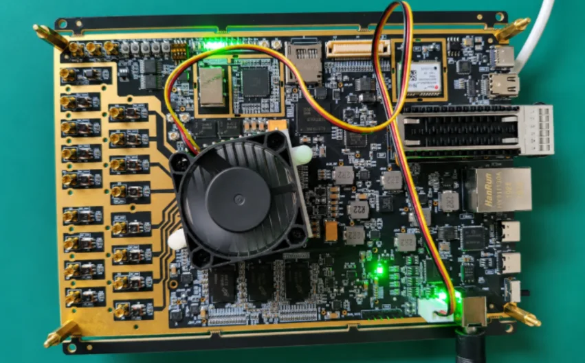
RFSoC Board PCB Manufacturing and Assembly One-Stop Service
Highleap Electronics supports customer-designed RFSOC...
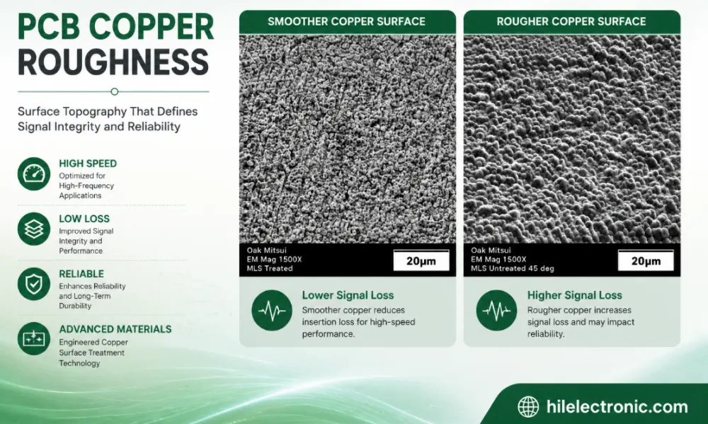
PCB Copper Roughness: Signal Loss, Material Selection and Manufacturing Control
Table of contentsWhat Is PCB Copper Roughness?How Copper...
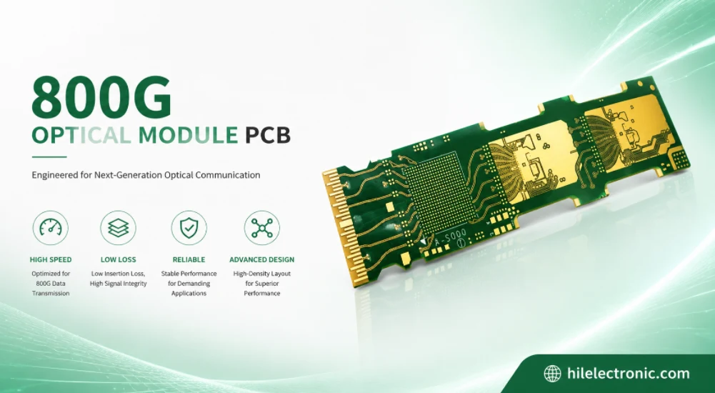
800G Optical Module PCB Manufacturing and Assembly Service
Table of contentsWhat Makes an 800G Optical Module PCB...
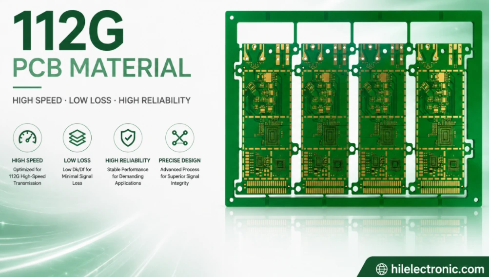
112G PCB Material Selection and High-Speed PCB Manufacturing
Table of contentsWhat “112G PCB Material” Actually...
How to get a quote for PCBs
Let us run DFM/DFA analysis for you and get back to you with a report.
You can upload your files securely through our website.
We require the following information in order to give you a quote:
-
- Gerber, ODB++, or .pcb, spec.
- BOM list if you require assembly
- Quantity
- Turn time
In addition to PCB manufacturing, we offer a comprehensive range of electronic services, including PCB design, PCBA (Printed Circuit Board Assembly), and turnkey solutions. Whether you need help with prototyping, design verification, component sourcing, or mass production, we provide end-to-end support to ensure your project’s success. For PCBA services, please provide your BOM (Bill of Materials) and any specific assembly instructions. We also offer DFM/DFA analysis to optimize your designs for manufacturability and assembly, ensuring a smooth production process.