
Back to blog
What is Multilayer PCB: manufacturing and design

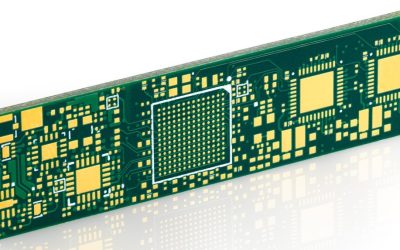
Unlike single-layer or double-layer PCBs, multilayer PCBs consist of three or up to 60 layers of copper, separated by insulating materials and laminated together under heat and pressure. These additional layers allow for more complex and dense circuit designs, accommodating a greater number of components on a smaller board. This capability is crucial in modern electronics, where devices are becoming increasingly compact yet more powerful. The evolution of multilayer PCBs has been driven by the demand for more efficient, reliable, and miniaturized electronic products.
Common Multilayer Constructions
- 4-6 layers – low to moderate complexity
- 8-10 layers – more complex digital boards
- 12-16 layers – advanced RF and data processing
- 20+ layers – extremely dense interconnections
- 60+ layers – state of the art HDI technology
Manufacturing Process of Multilayer PCBs
1. Inner Layer Formation
Photolithographic patterning is applied to copper-clad laminates to define the circuit traces, followed by etching away unwanted copper, adding layer registration targets and tooling holes, electrical testing of the traces, and surface preparation for lamination.
2. Layer Lamination
Multiple layers are bonded using sheet lamination presses, with a stackup arrangement of cores, prepregs, copper, and dielectrics, cured under temperature and pressure to form a solid laminate.
3. Drill Holes
High precision drilling creates tooling and via holes with accurate registration for each layer.
4. Hole Plating
Electroless copper plating followed by electrolytic copper plating builds up copper on the inner layers and drilled holes.
5. Outer Layer Processing
Application of liquid photoimageable solder mask, printing of identification markings, patterning and etching of outer layer circuitry, and routing of the panel into individual PCBs.
6. Testing and Quality Assurance
Includes automated optical inspection, net connectivity testing, impedance, high voltage, and functional testing, along with dimensional quality control.
Multilayer PCB Design Considerations
Number of Layers:
Deciding the number of layers is the first step in multilayer PCB design. The layer count, which can range from four to ten or more layers, depends on the complexity of the design, component count, and electrical performance requirements.
Component Placement
Using PCB layout software, designers arrange components and define electrical connections. The arrangement should optimize signal routing, minimize interference, and ensure heat dissipation.
Signal Routing
Electrical routing involves specifying the width, spacing, and layer assignment of connections, focusing on signal integrity, reducing cross-talk, and preventing signal reflection.
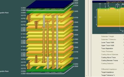
Layer Stacking Considerations:
The layers should be stacked with even numbers preferred, and all signal layers should be as close to the ground plane as possible. The direction of wiring on the same signal layer should be consistent. The choice of the number of layers also depends on the type of signal they need to transmit, categorized as high frequency, low frequency, ground, or power.
Component and Interface Arrangement:
Ideally, components should be placed on one side, and the position and orientation of interface components should be arranged reasonably. Components with close electrical connections are best placed together.
Gerber File Generation:
Once electrical routing is defined, Gerber files are generated, containing information about the layer stack-up, electrical connections, component placement, and other design information.
Manufacturing:
The manufacturer uses the Gerber files to create photomasks, which are then used to create individual PCB layers. These layers are laminated to form the final multilayer PCB.
Signal Integrity Considerations of Multilayer PCB
Layer Stack-Up: Properly planning the layer stack-up is crucial. Signal and ground layers should be closely coupled to minimize impedance and signal reflection.
Trace Routing: Traces should be routed to avoid crosstalk and electromagnetic interference (EMI). Keeping signal paths short and direct improves signal integrity.
Impedance Control: Maintaining consistent impedance across the PCB prevents signal distortion and reflections.
Decoupling Capacitors: These are essential for managing power integrity and minimizing noise on power planes.
Via Design: The design and placement of vias impact signal paths and should be optimized to maintain signal integrity.
Cost Considerations of Multilayer PCB
Complexity and Layer Count: More layers and complexity in design increase the manufacturing cost.
Materials Used: High-quality or specialized materials can raise the overall cost.
Manufacturing Techniques: Advanced manufacturing techniques for complex designs can also add to the cost.
Size of the PCB: Larger PCBs require more materials and processing, increasing the cost.
Quantity: Larger production runs can reduce the cost per unit due to economies of scale.

Related Articles
Why Is Immersion Gold and Gold Plating Needed on PCBs?
the gold plating process can be divided into two types: electroplated gold and immersion gold. For the gold plating process, its soldering effect is greatly reduced, while the soldering effect of immersion gold is relatively better.
Impedance Matching Meaning in High-Speed PCB Layout
A clear explanation of impedance matching in high-speed PCB layout, including why it matters, how stackup and routing affect it, and what to specify for fabrication.
In-depth Overview of PCB Laminate Construction
Understanding these PCB Laminate Construction is essential for PCB designers and manufacturers to create efficient and high-quality circuit boards.