
Back to blog
In-depth Overview of PCB Laminate Construction

PCB Laminate Construction
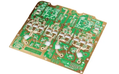
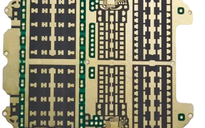
PCBs are the backbone of modern electronics, providing a platform for various components to connect and function seamlessly. At the core of every PCB lies a complex structure of interconnected layers, each serving a specific purpose in ensuring the board’s functionality and reliability.Among the key elements that a PCB Laminate Construction, stack-up diagrams play a pivotal role in defining the board’s construction and electrical properties. Understanding these PCB Laminate Construction is essential for PCB designers and manufacturers to create efficient and high-quality circuit boards.
The essence of a Printed Circuit Board (PCB) lies in its intricate structure that involves several layers interconnected by Prepregs and Core materials.
Prepreg, often referred to as B-stage resin-impregnated sheets, is a partially cured material composed of resin soaked into thin films. It serves dual purposes in multi-layer PCB manufacturing: it acts as an adhesive for bonding the inner conductive patterns and provides interlayer insulation. During lamination, Prepreg’s epoxy resin melts, flows, and solidifies, effectively merging the circuit layers while forming a reliable insulating barrier between them.
Core material, on the other hand, constitutes the foundational element of a PCB—a rigid board with a specific thickness and copper foil laminated on both sides. A typical multi-layer PCB is fabricated through the lamination of alternating layers of core and Prepregs. The Prepreg layers, which form what we call “wet-out” or impregnation layers, can bond multiple core layers together, and despite having an initial thickness, they experience some shrinkage during the pressing process.
Typically, the outermost two dielectric layers of a multilayer PCB are impregnation layers, covered by separate copper foil layers serving as external conductive planes. The raw thickness specifications for outer and inner copper foils commonly come in 0.5OZ, 1OZ, and 2OZ varieties (with 1OZ being approximately 35um or 1.4mil). Post-processing, the outer copper foil layer typically increases in thickness by nearly 1 OZ, while the final thickness of the inner copper foil remains close to the original value but may reduce slightly due to etching.
The outermost layer of a multilayer PCB consists of the soldermask, colloquially known as “Green Oil,” although it can also be yellow or other colors. The soldermask thickness is not easily determined precisely, being thicker in areas without copper compared to those with copper, yet the protrusion of the copper is still noticeable upon tactile inspection of the PCB surface.
PCB Parameters and Materials
Differences in PCB parameters exist among different manufacturers, necessitating communication with PCB factory engineers to obtain their specific data, primarily focusing on the dielectric constant and soldermask thickness, which can vary from one manufacturer to another.
Outer Layer Copper Foil Available outer layer copper foil thicknesses include 12um, 18um, and 35um. After processing, these generally result in final thicknesses of about 44um, 50um, and 67um, roughly equivalent to 1 OZ, 1.5 OZ, and 2 OZ copper weights respectively. Note that when using impedance calculation software for control, there is no option for 0.5 OZ copper thickness for outer layers.
Core Material Commonly used core material is S1141A, which is standard FR-4 material, double-sided copper-clad, with selectable specifications that can be confirmed directly with the manufacturer.
Prepreg Prepregs come in various original thickness specifications such as 7628 (0.185mm/7.4mil), 2116 (0.105mm/4.2mil), 1080 (0.075mm/3mil), and 3313 (0.095mm/4mil). Upon actual compression, the thickness usually decreases by around 10-15um (0.5-1mil), hence the minimum dielectric layer thickness in a stackup design must not be less than 3mil. A single impregnation layer can use up to three Prepregs, where none of the three can have identical thicknesses; at least one Prepreg can be used, though some manufacturers require a minimum of two. If the Prepreg’s thickness is insufficient, the copper foil on both sides of the core can be etched away and then reattached with Prepregs, achieving a thicker impregnation layer. The dielectric constant of Prepregs varies with their thickness, and the following table lists different models’ thicknesses and their corresponding dielectric constants:
| Model | Thickness (in mil) | Dielectric Constant |
|---|---|---|
| 1080 | 2.8mil | 4.3 |
| 3313 | 3.8mil | 4.3 |
| 2116 | 4.5mil | 4.5 |
| 7628 | 6.8mil | 4.7 |
The dielectric constant of a laminate board depends on the resin material used; FR4 boards typically exhibit a dielectric constant range of 4.2 to 4.7, which decreases with increasing frequency.
Soldermask Layer The thickness of the soldermask layer above the copper foil, denoted as C2, is approximately 8-10um. The thickness of the soldermask in areas without copper, C1, varies based on the surface copper thickness, being around 13-15um for 45um thick copper and around 17-18um for 70um thick copper. When calculating with SI9000, a soldermask thickness value of 0.5OZ suffices.
Conductor Cross-section Due to etching, the cross-section of conductors is not rectangular but rather trapezoidal. For example, in the TOP layer, when the copper foil thickness is 1OZ, the upper base of the trapezoid is about 1MIL shorter than the lower base. Thus, if the designed line width is W=5MIL, the upper width would be approximately 4MIL and the lower width 5MIL. The difference between the upper and lower bases is related to the copper thickness, as shown in the table below under different conditions:
| Line Width | Copper Thickness (OZ) | Upper Width (mil) | Lower Width (mil) |
|---|---|---|---|
| Inner Layer | 0.5 | W – 0.5 | W |
| Inner Layer | 1 | W – 1 | W |
| Inner Layer | 2 | W – 1.5 | W – 1 |
| Outer Layer | 0.5 | W – 1 | W |
| Outer Layer | 1 | W – 0.8 | W – 0.5 |
| Outer Layer | 2 | W – 1.5 | W – 1 |
| Note: W represents the ideal line width as designed. | |||
Impedance Calculations Typical impedance calculations employ the following models:
- Microstrip Line Model
- Stripline Model

In the microstrip model, other configurations exist, including an unused model without coating. The dielectric constants Er1 and Er2 in the illustrated model depend on the specific prepreg model used; key models are listed previously and detailed parameters should be obtained directly from the PCB manufacturer.
When the project moves from research to an RFQ, review PCB laminate selection and fine-pitch BGA assembly so the material, process, and inspection requirements stay aligned.
Overall,understanding the intricate structure and materials of a Printed Circuit Board (PCB) is crucial for designing and manufacturing high-quality electronic devices. Prepreg and Core materials play essential roles in bonding layers and providing insulation, while copper foils and soldermasks contribute to the PCB’s conductivity and protection.
Differences in PCB parameters and materials among manufacturers highlight the importance of communication and obtaining specific data for each project. Stack-up diagrams serve as invaluable tools, providing a blueprint of the PCB’s construction and electrical properties.
By comprehending the key elements of stack-up diagrams, designers can ensure the integrity and reliability of their PCB designs, ultimately leading to better-performing and more robust electronic devices.
PCB & PCBA Quick Quote
Related Articles
Rogers 5880 Laminates vs Other High-Frequency Materials
Highleap Electronics provides custom PCB manufacturing and assembly using Rogers 5880 Laminates and other high-frequency materials for 5G, automotive radar, and more.
China’s Leading Manufacturers for Rogers 5880 High-Frequency Circuit Boards
Get low-loss, signal integrity solutions for 5G, automotive radar, and satellite communications from Highleap Electronics.

Fast Turn Rigid Flex PCB: Accelerating Your Product Development
Accelerate innovation with Highleap Electronics’ fast turn rigid flex PCB solutions. Get rapid prototypes, precision fabrication, and reliable delivery for complex designs.