
Back to blog
The Advantages and Applications of Gold Plated PCBs

Gold Finger PCB
In the intricate and ever-evolving world of electronics, PCBs form the backbone of countless devices. Among the various advancements in PCB technology, gold plated PCBs have emerged as a standout solution, offering a blend of reliability, performance, and precision. This article aims to explore the multifaceted world of these specialized PCBs.
What are Gold Plating PCBs
Gold plated PCBs refer to PCBs that have a thin layer of gold applied to parts of their surfaces, particularly the pads and contacts. This gold plating is not just for aesthetics; it plays a crucial role in the functionality of the PCB. Historically, the use of gold in PCBs has been driven by the metal’s excellent conductive properties and its resistance to oxidation and corrosion. These attributes make gold an ideal choice for maintaining long-term performance in a variety of environments.
The process of applying gold to PCBs, often referred to as gold plating, involves several intricate steps which ensure the durability and efficacy of the PCBs in electronic components. Additionally, there are different types of gold plating used in PCBs, each with its unique characteristics and applications. Understanding these types is essential for selecting the right PCB for a specific application.
The Gold Plating Process in PCBs
The process of gold plating on Printed Circuit Boards (PCBs) is a critical aspect that endows these boards with their distinct properties. Understanding this process provides insight into why gold plated PCBs are highly valued in electronics.
1. Surface Preparation
Cleaning and Smoothing: Before gold plating, the PCB surface must be thoroughly cleaned and smoothed. Any contaminants or irregularities can adversely affect the adhesion and quality of the gold plating.
Micro-etching: A micro-etching process is often used to slightly roughen the surface, enhancing the gold’s adherence to the underlying copper.
2. Base Layer Plating
Nickel Plating: In most cases, a layer of nickel is first plated onto the PCB. Nickel serves as a barrier to prevent gold from diffusing into the copper and provides a surface for the gold to adhere to.
Uniformity and Thickness: This nickel layer must be uniform in thickness and free from defects to ensure the quality and longevity of the gold plating.
3. Gold Plating
Pre-Plating Preparation
Surface Cleaning: The initial step involves thorough cleaning of the PCB surface to remove any contaminants. This is typically achieved using a series of chemical baths that rid the surface of oils, dirt, and oxidation products.
Microscopic Surface Etching: Following cleaning, a mild acid solution is often used for etching the surface. This process creates a slightly rough texture on a microscopic level, which aids in the adhesion of the subsequent metal layers.
Nickel Underlayer Application
Electroless Nickel Plating: Prior to gold plating, a layer of nickel is deposited. This is usually done using an electroless plating process, which, unlike traditional electroplating, does not require an electric current.
Barrier Properties of Nickel: Nickel acts as a barrier to prevent the diffusion of copper into the gold layer. This is crucial as copper diffusion can lead to oxidation, compromising the PCB’s electrical properties.
Detailed Gold Plating Process
Immersion Gold Plating: The actual gold plating is typically done using an immersion process. The PCB is immersed in a bath containing gold salts and other chemicals. Through a displacement reaction, a thin layer of gold is deposited on the nickel layer.
Thickness Control: Controlling the thickness of the gold layer is critical. For most applications, the gold layer is kept thin, often just a few microinches thick. This is sufficient to provide the necessary surface properties without being prohibitively expensive.
Post-Plating Inspection and Quality Control
Thickness Measurement: After plating, the thickness of the gold layer is measured using techniques like X-ray fluorescence or coulometric thickness testing.
Adhesion Testing: To ensure the gold layer adheres well to the nickel, various adhesion tests, such as tape tests, are performed.
Advantages of Gold Plated PCBs
Gold plated PCBs are not just recognized for their aesthetic appeal; they offer a host of advantages that make them highly sought after in the electronics industry. This section delves into these benefits, highlighting how they outperform other PCB finishes.
1. Enhanced Electrical Conductivity
- Gold is renowned for its excellent electrical conductivity. A gold plated PCB, therefore, offers superior performance, especially crucial in high-speed and high-frequency applications.
- The uniformity of the gold plating ensures consistent signal integrity, an essential factor in complex and precision electronic devices.
2. Exceptional Corrosion Resistance
- Gold’s resistance to oxidation and corrosion is one of its most significant advantages. This property ensures that gold plated PCBs maintain their integrity and functionality over time, even in harsh environments.
- Their resistance to moisture makes them ideal for use in humid conditions, where other PCB finishes might fail.
3. Increased Durability
- Gold plating provides a hard and durable surface, making these PCBs less prone to wear and tear during handling and operation.
- The durability of gold plated PCBs makes them particularly suitable for applications where connectors are repeatedly plugged and unplugged.
4. Superior Solderability and Connectivity
- Gold plated surfaces offer excellent solderability, ensuring strong and reliable solder joints. This is vital for the overall robustness of the electronic assembly.
- The flatness and smoothness of the gold surface make it ideal for SMT, where precise placement of components is required.
Applications of Gold Plated PCBs
The remarkable qualities of gold plated PCBs extend their utility across a wide array of applications, marking their importance in various sectors of the electronics industry. This section explores the diverse uses of these PCBs, demonstrating their versatility and indispensability.
1. Consumer Electronics
- Smartphones and Computers: In devices like smartphones and laptops, gold plated PCBs are used for their reliability and superior electrical performance, essential for the functionality of these everyday devices.
- Wearables and High-End Audio Equipment: The corrosion resistance and consistent performance of gold plated PCBs make them ideal for wearables and high-end audio equipment, where long-term reliability is critical.
2. Industrial Applications
- Control Systems and Sensors: Gold plated PCBs are found in industrial control systems and sensors, where their durability and precision are crucial for accurate monitoring and control.
- Automotive Electronics: In the automotive sector, the robustness of gold plated PCBs supports the functioning of critical electronic systems in vehicles, which must endure various environmental stresses.
3. Medical Devices
- Diagnostic and Monitoring Equipment: Medical devices, particularly those used in diagnostics and patient monitoring, rely on gold plated PCBs for their consistent performance and reliability.
- Implantable Devices: The biocompatibility and corrosion resistance of gold make these PCBs suitable for implantable medical devices, where long-term stability is a necessity.
4. Aerospace and Military
- Satellite and Communication Systems: In aerospace applications, including satellites and communication systems, gold plated PCBs provide the required reliability and performance in extreme environmental conditions.
- Defense Equipment: The military sector employs gold plated PCBs in various high-tech equipment, valuing their durability and reliability in demanding situations.
5. Emerging Technologies
- Internet of Things (IoT) and AI: As the Internet of Things (IoT) and artificial intelligence (AI) technologies advance, gold plated PCBs are increasingly used for their ability to maintain signal integrity in complex circuits.
- 5G Technology: The high-frequency requirements of 5G technology make gold plated PCBs an ideal choice due to their superior electrical properties.
Conclusion
In the intricate and ever-evolving world of electronics, PCBs form the backbone of countless devices. Among the various advancements in PCB technology, gold plated PCBs have emerged as a standout solution, offering a blend of reliability, performance, and precision. Gold plated PCBs feature a thin layer of gold applied to specific parts of their surfaces, enhancing conductivity, corrosion resistance, and durability. The process involves multiple steps including surface preparation, nickel underlayer application, and controlled gold plating. These PCBs are highly valued in industries such as consumer electronics, industrial applications, medical devices, aerospace, military, and emerging technologies due to their superior qualities.
FAQ for Gold Plated PCBs
1. What distinguishes gold plated PCBs from other PCB finishes in terms of performance?
Gold plated PCBs are distinguished by their excellent electrical conductivity, corrosion resistance, and durability. These properties make them ideal for high-speed, high-frequency applications and environments where long-term reliability is critical.
2. How does the gold plating process ensure the longevity and efficiency of PCBs?
The gold plating process involves meticulous steps such as surface preparation, nickel underlayer application, and controlled gold deposition. These steps ensure that the gold adheres well, providing a durable and conductive surface that resists oxidation and wear.
3. In which industries are gold plated PCBs particularly advantageous, and why?
Gold plated PCBs are advantageous in industries such as consumer electronics, automotive, medical devices, aerospace, and defense due to their reliable performance, resistance to harsh environments, and superior electrical properties.
4. What are the key considerations when selecting gold plated PCBs for high-frequency applications?
When selecting gold plated PCBs for high-frequency applications, consider the uniformity of the gold layer, which ensures consistent signal integrity. The low resistance and high conductivity of gold also play a crucial role in maintaining performance in these demanding applications.
5. How does the use of gold plated PCBs impact the overall reliability of electronic assemblies?
Gold plated PCBs enhance the overall reliability of electronic assemblies by providing superior solderability, strong and reliable solder joints, and a durable surface that withstands repeated use and harsh conditions. This results in more robust and long-lasting electronic products.

Related Articles
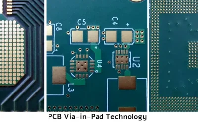
Comprehensive Analysis of PCB Via-in-Pad Technology
Explore the key advantages and challenges of Via-in-Pad technology in PCB design, with expert tips for maximizing performance and reliability.
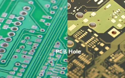
PCB Hole Selection to Optimize PCB Performance and Cost
Discover how to optimize your PCB designs with effective hole selection techniques like back drilling vs buried vias, mechanical vs laser drilling, and HDI stack planning to improve performance while minimizing manufacturing complexity and costs.
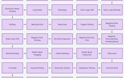
PCB Manufacturing Process Flow – Ultimate Guide Is Here
High-Quality PCB Manufacturing Solutions: Precision, Speed, and Reliability for Your Electronics Projects – From Prototype to Mass Production.
Take a Quick Quote