
Back to blog
What Is Automated Optical Inspection (AOI)?

Automated Optical Inspection (AOI) has become an indispensable technology in the field of Surface Mount Technology (SMT) for printed circuit board (PCB) assembly manufacturing, especially in regions with high-technology industries like the USA. This technology significantly contributes to maintaining high standards of quality control, thereby ensuring the reliability and functionality of PCBs across various applications, from consumer electronics to critical aerospace and medical devices.
Introduction to AOI in SMT PCB Assembly
AOI systems automate the visual inspection process that was traditionally done manually, offering a much faster, more accurate, and consistent inspection method. This automation is particularly valuable in high-mix manufacturing environments where the diversity of PCB designs and components can be vast, and the room for error is minimal.
Core Components of AOI Systems
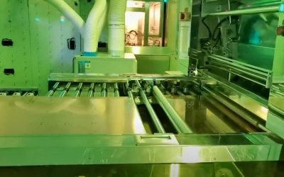
- High-Resolution Cameras: AOI machines are equipped with one or more high-resolution cameras that capture detailed images of the PCB. These cameras can be stationary or mobile, depending on the system design. Some systems use multiple cameras to capture images from different angles or to inspect various parts of the board simultaneously.
- Lighting Systems: Effective lighting is crucial for AOI. Different lighting systems (e.g., LED arrays) are used to illuminate the PCB from various angles, enhancing the visibility of components, solder joints, and potential defects. Lighting techniques, such as bright-field, dark-field, and side lighting, help highlight different types of features and flaws.
- Software Algorithms: The heart of AOI testing lies in its software, which analyzes the captured images. Advanced algorithms compare the images against predefined criteria or a digital “golden board” – a reference model of what the perfect PCB should look like. These algorithms can detect a wide range of defects by analyzing shapes, colors, and contrasts.
How AOI Works
- Setup and Calibration: Before testing can begin, the AOI system must be calibrated and programmed with the specific inspection criteria for the PCB being manufactured. This includes inputting the design specifications, component library, and acceptable tolerance levels for various features.
- Image Capture: As PCBs pass through the AOI machine, cameras capture images from different angles. This comprehensive imaging ensures that the system can inspect all aspects of the board, including component presence, placement accuracy, solder quality, and more.
- Image Analysis: The captured images are then analyzed by the software. Using complex algorithms, the system checks for various potential defects.
- Reporting and Feedback: After inspection, AOI systems generate detailed reports highlighting detected defects. This data is crucial for diagnosing process issues and implementing corrective measures. It also provides valuable feedback for continuous improvement in manufacturing processes.
Advanced Technologies Employed in AOI systems
2D and 3D Imaging: 3D imaging technologies, such as laser triangulation or structured light, complement traditional 2D imaging by providing detailed information on the height and volume of components and solder joints. This allows for more accurate detection of defects related to component placement and solder quality.
This page is the definition-level AOI guide. For how AOI is applied inside PCB and PCBA production, use AOI for PCB and PCBA inspection; for broader inspection and documentation control, review Highleap’s PCB quality assurance process.
Machine Learning and AI: Some AOI systems incorporate machine learning algorithms that improve defect detection over time. These systems learn from past inspections, enhancing their ability to distinguish between true defects and permissible variations in the manufacturing process.
Integration with SMT Equipment: Modern AOI systems are often integrated with other SMT equipment, allowing for real-time feedback and adjustments. This integration helps in quickly identifying issues and reducing the incidence of defects downstream in the PCB assembly process.
Types of Defects Detected
The versatility of AOI systems allows for the detection of a wide variety of defects:
- Missing Parts: Identified through 2D imaging, with 3D imaging providing additional clarity in low-contrast situations.
- Polarity and Part Numbers: Verifies that components are placed with the correct orientation and matches the bill of materials.
- Positional Defects: Detects shifts or misalignments, grading them according to established IPC standards.
- Physical Anomalies: Such as tombstoning, bent or lifted leads, and various soldering defects (e.g., open circuits, shorts, insufficient solder).
- Coplanarity Verification: Essential for ensuring the flatness of critical components like BGAs, utilizing 3D imaging for accuracy.
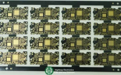
AOI in Practice at Highleap Electronic
At Highleap Electronic, a hypothetical high-mix PCB manufacturing facility, AOI is a core part of the quality assurance process. The technology is employed post-SMT pick-and-place and reflow soldering processes to identify and flag any defective boards for rework, providing clear imagery of the detected issues for quick resolution. Furthermore, AOI is crucial for solder paste inspection, ensuring proper coverage and quality before proceeding with component placement, which is critical for the success of the initial job setup and the introduction of new solder paste batches.

Related Articles
How PCB Dry Film Plays a Key Role in Enhancing PCB Reliability
Revolutionize your PCB manufacturing with our cutting-edge PCB dry film technology!
High-Quality Rigid PCB Circuit Board Fabrication Services
Rigid PCBs are the conventional type of FR4 PCB, comprising a rigid substrate typically made of materials like fiberglass.
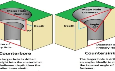
PCB Mounting Holes: Understanding Counterbore and Countersink
The choice between countersink and counterbore holes depends on various factors, including the type of screw and the application requirements.