
Back to blog
PCB for Beginners: Employment Opportunities and Manufacturing Processes

What is a Printed Circuit Board?
A Printed Circuit Board (PCB) is a rigid structure that supports and electrically connects electronic components using embedded metal surfaces called traces and planes. Components are soldered onto metal pads on the board, allowing for electrical connections and interaction between components. PCBs can be single-sided, double-sided, or multi-layered, depending on the complexity required.
Substrate (Base Material): The substrate, or base material, of a PCB is typically composed of FR-4, a flame-resistant composite made of woven fiberglass cloth and epoxy resin. This material provides the necessary structural support and insulation for the board, ensuring that the electrical signals do not interfere with each other. The rigidity and durability of FR-4 make it the most common choice for PCB substrates, allowing the board to withstand various environmental conditions and mechanical stresses.
Copper Layer: The copper layer of a PCB consists of thin layers of copper foil that form the conductive pathways, or traces, responsible for carrying electrical signals between components. These traces are etched from the copper foil laminated onto the substrate. The copper layer’s quality and thickness are crucial, as they determine the board’s electrical conductivity and the ability to handle different current loads. Multiple copper layers can be used in more complex, multi-layered PCBs to accommodate intricate circuit designs.
Solder Mask: The solder mask is a protective polymer layer applied over the copper traces of a PCB. Its primary function is to prevent short circuits and oxidation of the copper traces, ensuring the board’s reliability and longevity. The solder mask also helps in the soldering process by preventing solder bridges between closely spaced solder pads. Typically green in color, solder masks are available in various colors to meet different aesthetic and functional requirements.
Silkscreen: The silkscreen layer is the top layer of a PCB, printed with ink to display text and symbols. This layer provides essential information for component identification and assembly guidance, such as component labels, part numbers, and other critical markings. The silkscreen helps engineers and technicians during the manufacturing, assembly, and troubleshooting processes, ensuring that components are placed and connected correctly.
Key Employment Opportunities in the PCB Industry
The PCB industry offers a wide range of core employment opportunities essential for the design, production, and support of printed circuit boards. Some of the key job roles include PCB Design Engineer, Electrical Engineer, Manufacturing Engineer, Quality Control Engineer, Test Engineer, Process Engineer, Procurement Specialist, Supply Chain Manager, Sales Representative, Marketing Specialist, Customer Support Technician, After-Sales Service Engineer, Research and Development Engineer, Project Manager, Industrial Designer, Production Manager, Materials Manager, Equipment Maintenance Technician, Assembly Line Worker, Compliance Officer, CAD Technician, and Layout Engineer.
These roles are crucial for the successful lifecycle of PCB production, from initial concept and design through to manufacturing, quality assurance, and market deployment. Professionals in these positions collaborate to ensure the efficient creation of high-quality PCBs that meet industry standards and client requirements. The industry offers significant opportunities for specialization and advancement, drawing on diverse expertise from engineering, technical, management, and operational backgrounds.

Why Do We Manufacture PCBs?
Printed Circuit Boards (PCBs) are at the heart of modern electronics, ensuring our devices work seamlessly and reliably. We manufacture PCBs because they provide efficient and precise electrical connections between components. Imagine the chaos of manually wiring every component in a smartphone or computer – it would be a nightmare of errors and impracticality. PCBs streamline this process, ensuring electrical signals are routed correctly, which significantly enhances the performance and reliability of our electronic devices.
Without PCBs, the electronics we depend on daily would be bulky, unreliable, and incredibly complex to produce. The compact and organized layout that PCBs offer is essential for modern devices, allowing them to be smaller and more efficient. This organization makes mass production feasible, reducing costs and ensuring consistent quality across products. The reliability provided by PCBs translates to fewer failures and longer device lifespans, which is critical for applications where performance consistency is vital, such as in medical equipment and aerospace technology.
Moreover, PCBs improve signal integrity and reduce electrical noise, crucial for high-speed and high-frequency applications. Their versatility allows their use across various industries, from consumer electronics to automotive and aerospace. If we didn’t manufacture PCBs, our ability to innovate and advance technology would be severely limited. Devices would be larger, more expensive, and prone to frequent failures. The standardized yet customizable nature of PCBs ensures we can meet specific design requirements while adhering to environmental and safety standards, promoting sustainable development. In essence, without PCBs, the seamless functionality and rapid advancement of electronic technology would grind to a halt.
Which PCB-Related Field Holds the Most Learning Potential?
In the dynamic and ever-evolving field of PCB technology, certain specializations stand out due to their significant impact on the industry and the opportunities they present for innovation and career growth. Among these, the field of PCB Design Engineering holds the most potential for learning and advancement.
PCB Design Engineering
PCB Design Engineering is at the forefront of PCB development, responsible for creating the layout of the board, placing components, and ensuring that electrical connections are efficient and reliable. This specialization is critical for several reasons:
- PCB Design Engineers are often tasked with solving complex problems and developing new design methodologies to meet the increasing demands for smaller, faster, and more efficient electronic devices. The need for innovative solutions makes this field exciting and continually challenging.
- With the rise of technologies such as 5G, Internet of Things (IoT), and advanced computing, PCB designs are becoming more intricate and sophisticated. Design engineers must stay updated with the latest tools and techniques, making continuous learning an integral part of their career.
- The demand for skilled PCB Design Engineers is consistently high across various industries, including consumer electronics, automotive, aerospace, and communication. This demand ensures that professionals in this field have numerous job opportunities and the potential for career advancement.
- PCB Design Engineering requires a blend of knowledge from electrical engineering, materials science, and computer-aided design (CAD) software. This interdisciplinary approach enriches the learning experience and broadens the engineer’s skill set.
- PCB Design Engineers play a crucial role in the product development lifecycle. Their work directly influences the performance, reliability, and manufacturability of electronic products. This impact on the final product is both rewarding and motivating for professionals in the field.
Diverse Roles within PCB Design Engineering
PCB Design Engineering encompasses several specialized roles, each contributing uniquely to the development and optimization of PCBs. Embedded Systems Engineers integrate software and hardware to create efficient and functional embedded systems, often working closely with PCB design to ensure seamless integration of microcontrollers and other embedded components. Hardware Engineers focus on the physical aspects of electronic devices, designing and testing the circuits that make up the PCB, ensuring that they meet the required specifications and performance standards. Signal Integrity Engineers are specialized in analyzing and mitigating issues related to signal transmission, ensuring that the PCB design supports high-speed data communication without interference or loss. These roles highlight the broad and diverse nature of PCB Design Engineering, making it a field ripe with opportunities for specialization and career growth.
PCB Design Engineering stands out as the most promising field within PCB-related professions due to its blend of innovation, technological advancements, high demand, interdisciplinary nature, and significant impact on product development. For those seeking a dynamic and rewarding career with ample opportunities for learning and growth, PCB Design Engineering offers a pathway to becoming a pivotal player in the electronics industry.

How to Get Started with Learning PCB Design
Learning PCB design can be a rewarding endeavor, opening up numerous career opportunities in various industries. Here’s a step-by-step guide to help you get started with PCB design:
1. Understand the Basics of Electronics
Before diving into PCB design, it’s crucial to have a solid understanding of basic electronics. This includes knowledge of electrical components such as resistors, capacitors, inductors, diodes, transistors, and integrated circuits (ICs). Familiarize yourself with fundamental concepts like Ohm’s Law, Kirchhoff’s laws, and basic circuit analysis. These concepts form the foundation of all electronic circuit design and are essential for understanding how to connect and troubleshoot components on a PCB.
To build this foundational knowledge, you can utilize a variety of resources. Online courses from platforms like Coursera, edX, and Khan Academy offer comprehensive introductions to electronics. Additionally, textbooks such as “The Art of Electronics” by Paul Horowitz and Winfield Hill provide in-depth explanations and practical examples. These resources will help you grasp the basics and prepare you for more advanced PCB design concepts.
2. Learn Schematic Capture
Schematic capture is the process of creating a diagram that represents the electrical connections between components. It is an essential skill for PCB design. Choosing a schematic capture tool is the first step; popular options include KiCAD, Eagle, and Altium Designer. These tools allow you to draw schematics, place components, and define the electrical connections (nets) between them.
Start with simple projects to get familiar with the tool’s interface and functionality. Practice by designing basic circuits, such as a simple LED blink circuit or a power supply. This hands-on experience is invaluable. Online tutorials and videos can guide you through the process, and documentation or user guides provided by the software developers can help you troubleshoot and learn advanced features.
3. Get Familiar with PCB Layout Software
PCB layout involves arranging the physical components on the board and routing the electrical connections. Learning to use PCB design software is crucial. Popular software includes KiCAD, Eagle, and Altium Designer, each offering different features suitable for various levels of complexity and project sizes. KiCAD is free and open-source, Eagle is free for small projects, and Altium Designer is a professional, feature-rich option.
To get started, install your chosen software and explore its interface. Begin with simple designs to practice component placement and trace routing. Understanding design rules and constraints, such as trace width and spacing, is vital for creating functional and reliable PCBs. Utilize software-specific tutorials, forums, and online courses on platforms like YouTube and Udemy to deepen your understanding and improve your skills.
4. Study Design Principles and Best Practices
Learning the principles and best practices of PCB design ensures that your designs are efficient, reliable, and manufacturable. Key concepts include signal integrity and minimizing electromagnetic interference (EMI), which are crucial for high-speed and high-frequency applications. Proper power distribution and grounding techniques are also essential for stable operation, while thermal management helps prevent overheating and ensures longevity.
Resources such as articles and whitepapers from PCB manufacturers can provide insights into these best practices. Books like “PCB Design for Real-World EMI Control” by Bruce Archambeault offer detailed guidance on handling design challenges. Understanding and applying these principles will help you create robust and effective PCB designs.
5. Work on Practical Projects
Applying what you’ve learned through practical projects is one of the best ways to gain experience. Start with small, simple projects like creating a basic LED circuit or a power supply. These projects help reinforce your understanding of schematic capture and PCB layout while allowing you to practice soldering and assembly skills.
As you gain confidence, progress to more complex projects, such as microcontroller-based designs or sensor circuits. Document your projects thoroughly and seek feedback from online communities. This practice not only improves your technical skills but also helps build a portfolio that can be useful for job applications or freelance work. Project kits from electronics stores like Adafruit and SparkFun, as well as online tutorials from platforms like Instructables and Hackster.io, can provide inspiration and guidance.
6. Join Online Communities and Forums
Joining online communities allows you to learn from experienced designers, ask questions, and share your projects. These communities are a valuable resource for troubleshooting, advice, and networking. Popular communities include Reddit’s /r/electronics and /r/PCB, Stack Exchange’s Electronics section, and EDA-specific forums like KiCAD.info and EEVblog.
Engaging with these communities can provide real-world insights and solutions to common design challenges. You can also find collaborative opportunities and stay updated on industry trends and new technologies. Regular participation in these forums can significantly enhance your learning experience and professional growth.
7. Consider Formal Education or Certifications
If you want to deepen your knowledge, consider formal education or certifications in electronics or PCB design. Enrolling in a degree program in Electrical Engineering or a related field can provide a comprehensive understanding of the theoretical and practical aspects of electronics. These programs often include courses on circuit design, signal processing, and embedded systems, which are directly applicable to PCB design.
Alternatively, specialized courses in PCB design offered by professional organizations or institutions can provide focused training. Certifications from recognized institutions, such as IPC Designer Certification, validate your skills and knowledge, making you a more competitive candidate for job opportunities. These formal qualifications can open doors to advanced roles and specialized fields within the PCB industry.
8. Practice, Practice, Practice
The key to mastering PCB design is consistent practice. Continuously challenge yourself with new projects and stay updated with the latest trends and technologies in the field. Regularly working on different types of projects helps you gain a deeper understanding of various design techniques and problem-solving strategies.
Stay curious and proactive in learning. Follow industry news, attend webinars, and participate in workshops to keep your skills current. By maintaining a practice-oriented approach and leveraging available resources, you can develop a strong foundation in PCB design and pave the way for a successful career in the electronics industry.
Introduction to PCB Types, Key Components, and Materials
PCB Types
Rigid PCBs are the most common type, known for their sturdy and durable structure, and are widely used in various electronic devices due to their reliable electrical connections and stability. Flexible PCBs use a flexible base material, allowing the board to bend and twist during use, making them suitable for applications with limited space or where dynamic flexing is required, such as wearable devices and flexible displays. Rigid-flex PCBs combine the advantages of both rigid and flexible PCBs, featuring rigid sections for support and flexible sections for flexibility, making them ideal for complex designs like foldable phones and medical devices.
High-frequency PCBs are specifically designed for high-frequency signal transmission and are used in wireless communications, radar systems, and high-frequency measurement equipment, utilizing special materials and design techniques to ensure signal integrity and minimize loss. Multilayer PCBs consist of multiple layers of conductive material and insulation, suitable for complex circuit designs such as computer motherboards and high-performance servers, allowing for higher circuit density and more compact designs.
Key Components and Materials
Understanding the key components and materials used in PCBs is essential for appreciating their functionality and design. The primary materials and components contribute to the PCB’s structural integrity, electrical performance, and overall reliability.
Key components and materials include:
- Substrate materials: FR-4, PTFE, and ceramics.
- Copper cladding: Various types and thicknesses of copper layers.
- Surface finishes: HASL, ENIG, and OSP.
- Components: Resistors, capacitors, diodes, transistors, and integrated circuits (ICs).
Introduction to PCB Design and Manufacturing Processes
Understanding PCB types, key components, and materials is essential, but grasping the PCB design and manufacturing processes is equally important. PCB design involves creating schematics and physical layouts, while PCB manufacturing covers everything from substrate material selection to final testing. To dive deeper into these processes, you can refer to the following linked articles:
These resources will provide you with a comprehensive understanding of the entire journey from concept to finished product, ensuring that every step of the design and manufacturing process meets high-quality and reliability standards.
Conclusion
Through the above content on PCBs, you now have a general understanding of what PCBs are, their types, key components, and materials. However, mastering PCB knowledge requires extensive practical experience. As you progress and feel confident in your PCB knowledge, you might want to embark on creating your own electronic projects. This is where Highleap Electronic comes in, offering comprehensive PCB solutions and turnkey PCBA services to support your endeavors.
Whether you’re a hobbyist looking to bring your ideas to life or a professional seeking reliable PCB manufacturing and assembly, Highleap Electronic provides the expertise and resources needed to ensure your projects succeed. From design to production and assembly, our services cover all aspects, allowing you to focus on innovation and creativity. Contact us today to learn how we can assist you in achieving your electronic project goals.

Related Articles
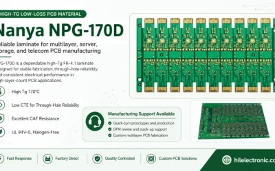
Nanya NPG-170D PCB Manufacturing for High-Tg Multilayers
Nanya NPG-170D PCB manufacturing for halogen-free high-Tg multilayers, including DR/DTL material callout, stackup, CAF control, lead-free assembly, testing, and RFQ data.
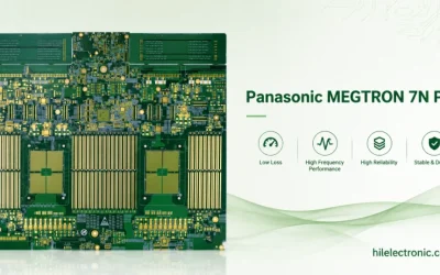
Panasonic MEGTRON 7N PCB Manufacturing for High-Speed HDI
Panasonic MEGTRON 7N PCB manufacturing for high-speed HDI and high-layer-count boards, covering R-5785(N), R-5680(N), loss budget, impedance, drilling, backdrill, and RFQ data.
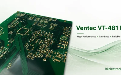
Ventec VT-481 PCB Manufacturing for Lead-Free Multilayers
Ventec VT-481 PCB manufacturing notes for lead-free multilayer boards: low Z-CTE, CAF control, stackup review, drilling, plating, assembly, and RFQ data.