
Back to blog
OSP Process Guidelines for PCB Manufacturing

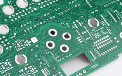
OSP PCB Technology
Organic Solderability Preservatives (OSP) technology stands at the forefront of innovation in the electronic manufacturing industry, particularly in PCB manufacturing. This surface treatment technology has garnered significant attention for its ability to enhance PCB performance and longevity. In this article, we will delve into the intricacies of OSP technology, exploring its principles, processes, advantages, and challenges.
Understanding the Principles of OSP PCB Technology
OSP PCB technology relies on the principle of forming a protective film on the PCB surface using an organic solder resist. This protective film, applied through coating methods like dipping or spraying, serves to shield the exposed copper surface from oxidation and contamination during manufacturing and transportation. The key principles of OSP technology can be broken down into the following steps:
- Surface Preparation: The exposed copper surface undergoes thorough cleaning and treatment to ensure proper adhesion of the organic solder resist, facilitating the formation of a uniform protective film.
- Organic Solder Resist Coating: Following surface preparation, the PCB is coated with an organic solder resist containing active substances that form chemical bonds with the copper surface, ensuring strong adhesion.
- Protective Film Formation: The organic solder resist forms a uniform protective film on the PCB surface, effectively preventing oxidation and corrosion without impacting electronic component functionality.
- Stripping During Welding: During PCB assembly, the organic solder mask protective layer is stripped off through heat treatment, ensuring the reliability of solder joints by revealing the exposed copper surface.
By employing these principles, OSP PCB technology enhances soldering performance and ensures the reliability of electronic components, laying the groundwork for its widespread application in electronic manufacturing.
Requirements for OSP PCB Production Process
OSP is a surface treatment technology used in PCB manufacturing to protect the copper surface from oxidation and contamination. To ensure the effectiveness of OSP treatment and the quality of PCB production, several key requirements must be followed throughout the production process:
- Incoming PCB Material Handling: Incoming PCBs should be vacuum-packed with a desiccant and humidity display card attached. During transportation and storage, use separator paper between OSP-coated PCBs to prevent surface damage. Avoid exposing PCBs to direct sunlight.
- Storage Environment: Maintain a good storage environment with a relative humidity of 30% to 70% and a temperature of 15°C to 30°C. The shelf life of OSP-coated PCBs should be less than 6 months.
- Unpacking and Inspection: At the SMT site, unpack OSP-coated PCBs carefully, checking the vacuum packaging, desiccant, and humidity display card. Unqualified boards should be returned to the manufacturer for rework. PCBs should be assembled within 8 hours of unpacking to avoid prolonged exposure.
- Production Process: After printing, PCBs should go through the furnace as soon as possible and not stay for more than 1 hour, as the flux in the solder paste can corrode the OSP film. Maintain a workshop environment with a relative humidity of 40% to 60% and a temperature of 18°C to 27°C.
- Handling During Production: Avoid touching the PCB surface directly with hands to prevent contamination by sweat and oxidation. After completing single-sided SMT, complete second-sided SMT component assembly within 12 hours.
- DIP Plug-in: After SMT, complete DIP plug-in in the shortest time possible, up to 24 hours. Moisture OSP PCBs cannot be baked, as high-temperature baking can cause discoloration and deterioration of OSP.
- Rework and Reuse: Overdue or damp OSP-coated PCBs that have not been used in production should be returned to the manufacturer for OSP rework and re-use. However, the same board cannot be reworked more than three times, after which it must be scrapped.
Adhering to these requirements ensures the integrity of OSP-coated PCBs throughout the production process, resulting in high-quality and reliable electronic products.
OSP PCB Technology Process Flow
The process flow of OSP PCB technology is crucial for achieving an even coating of the organic solder resist and forming a reliable protective film. The typical process flow includes the following key steps:
-
Surface Cleaning and Preparation: The exposed copper surface undergoes thorough cleaning and treatment to remove contaminants, ensuring good roughness and cleanliness.
-
Organic Solder Mask Coating: After surface preparation, the PCB is coated with an organic solder mask protectant, often containing active substances that form strong chemical bonds with the copper surface.
-
Protective Film Formation: Following the application of the organic solder resist, the PCB undergoes heating or drying to promote the formation of a uniform protective film, critical for preventing oxidation and corrosion.
-
Testing and Quality Control: The coated PCB is inspected to ensure the uniformity and quality of the organic solder mask and the protective film, using visual inspection, chemical analysis, and testing equipment.
-
Peeling Off During Welding: Heat treatment is applied to the area coated with organic solder mask protectant during the PCB assembly stage, causing it to peel off at the solder joints, ensuring the reliability of the welding joints.
Through these steps, OSP PCB technology effectively protects the PCB surface, improves welding performance, and enhances overall reliability.
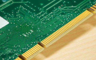
SMT Solder Paste Steel Mesh Design for OSP PCBs
OSP PCBs require specific design considerations for the steel mesh used in solder paste printing during Surface Mount Technology (SMT) assembly:
Enlarged Openings for Complete Pad Coverage:
Organic Solderability Preservative (OSP) PCBs benefit from a flat OSP surface for solder paste formation. However, pads alone may not provide sufficient solder. Therefore, it is essential to appropriately enlarge the openings in the steel mesh to ensure complete coverage of the entire pad. When transitioning a PCB from spray tin to OSP, the steel mesh must be reopened to accommodate this change.
Concave Design to Address Issues:
After enlarging the openings, consider changing the design of the solder paste printing stencil to a concave shape. This design adjustment can help resolve issues such as tin beads, tombstones, and exposed copper on OSP PCBs. Special attention should be given to preventing tin beads, which can lead to poor soldering quality.
Coverage for Unplaced Parts:
Even if certain parts are not placed on the PCB for any reason, it is crucial to ensure that the solder paste covers the pads as much as possible. This practice helps maintain uniformity in the soldering process and prevents oxidation of exposed pads, ensuring better overall reliability of the PCB.
Preventing Oxidation with Strategic Printing:
To further prevent the oxidation of exposed copper foil and potential reliability issues, consider strategically printing ICT test points, mounting screw holes, and exposed through holes with tin paste on the front side of the PCB. For areas designated for wave soldering on the reverse side, ensure these aspects are fully considered when designing the steel mesh openings.
Advantages and Challenges of OSP PCB Technology
Advantages of OSP PCB Technology
One of the primary advantages of OSP PCB technology is its ability to enhance welding performance. By reducing oxidation and pollution during the welding process, OSP technology ensures the creation of reliable and high-performance solder joints. This is crucial for the overall functionality and longevity of electronic devices. Additionally, OSP technology is known for its cost-effectiveness. Compared to traditional surface treatment methods, OSP is more economical due to its simpler process and lower material costs. This makes it an attractive option for manufacturers looking to reduce production expenses without compromising quality.
Environmental Friendliness and Wide Applicability
Another key advantage of OSP PCB technology is its environmental friendliness. OSP technology avoids the use of toxic metals, making it a more sustainable option that aligns with modern environmental protection requirements. Additionally, OSP technology offers wide applicability, making it suitable for various electronic components and circuit boards. This versatility is a significant benefit for manufacturers who need a surface treatment method that can adapt to different types of products and production processes.
Challenges Associated with OSP PCB Technology
Despite its many advantages, OSP PCB technology also faces several challenges. One of the main challenges is reliability issues related to the organic solder mask protective films. These films can be susceptible to mechanical stress during the peeling process, which can potentially affect the protection at welding points. Additionally, OSP PCB technology requires precise process control to ensure the uniform application of the organic solder mask and the formation of the protective film. This high level of process control adds complexity to the manufacturing process and requires careful monitoring to avoid performance issues.
Thermal Stability and Post-Welding Processing
Another challenge of OSP PCB technology is its limited thermal stability in high-temperature environments. This limitation can restrict its use in certain applications where exposure to high temperatures is a concern. Additionally, OSP technology requires a stripping process after welding, which adds complexity to the manufacturing process. Improper execution of this process can result in incomplete stripping, affecting the performance of the solder joint. Despite these challenges, OSP PCB technology remains a popular choice for manufacturers due to its many advantages and wide applicability.
Conclusion
OSP PCB technology offers a multitude of advantages, including improved welding performance, cost-effectiveness, environmental friendliness, and wide applicability. Despite facing challenges such as reliability issues and high process control requirements, OSP technology remains a highly beneficial surface treatment method in electronic manufacturing. By understanding and optimizing the principles and processes of OSP technology, manufacturers can enhance the reliability and performance of PCBs, meeting the demands of modern electronic manufacturing.

Related Articles
PCB Surface Preparation – A Complete Guide to Immersion Tin
In this detailed guide, we will explore the immersion tin plating process, its properties, applications, and comparisons with other common finishes.
Understanding PCB Laminate Materials: A Comprehensive Guide
The PCB lamination process is often misunderstood by circuit board users, leading to confusion about its purpose and significance. In this article, we aim to clarify the PCB lamination process and its importance in PCB manufacturing.
Gold Finger PCB Beginner’s Guide
This comprehensive guide delves into the intricacies of Gold Finger PCBs, from their composition and manufacturing processes to their diverse applications and impact on technology.