
Back to blog
Gold Finger PCB Beginner’s Guide

In today’s interconnected world of electronics, the transmission of signals between devices is more critical than ever. At the heart of this digital exchange lies a remarkable component known as the Gold Finger PCB. Serving as the linchpin between motherboards and secondary circuits, Gold Finger PCBs play a pivotal role in enabling seamless communication and functionality across a diverse array of electronic devices. This comprehensive guide delves into the intricacies of Gold Finger PCBs, from their composition and manufacturing processes to their diverse applications and impact on technology.
Understanding Gold Finger PCBs
Gold Finger PCBs, characterized by their gold-plated connectors along PCB edges, serve as essential conduits for electrical and data transmission between interconnected electronic components. Beyond computers, they are integral to the operation of smartphones, wearables, and various digital devices that rely on intricate signal pathways for functionality.
Crafted from flash gold, renowned for its durability and conductivity, Gold Finger PCBs undergo meticulous manufacturing processes to meet stringent specifications. Their thickness typically ranges from 3 to 50 microns, ensuring optimal performance and longevity in demanding applications.
The Role of Gold Plating in Gold Finger PCBs
Gold plating of PCB contact points is essential to enhance their durability and reliability amidst frequent insertion and ejection cycles. While gold may seem like a costly choice compared to alternatives like copper, its exceptional corrosion resistance, conductivity, and compatibility with alloying elements such as cobalt and nickel make it indispensable in the realm of Gold Finger PCB manufacturing.
Unlike silver, which is prone to chemical reactions and degradation, gold remains inert and stable over time, making it ideal for contact parts exposed to wear and tear. The process of gold plating strengthens the contact edges, ensuring seamless connectivity and optimal performance in electronic devices.
Manufacturing Process of Gold Finger PCBs
The manufacturing process of Gold Finger PCBs entails precision engineering and meticulous surface treatment to achieve superior quality and reliability. After soldering, gold plating is applied to the circuit board edges, typically following surface finishing to optimize adhesion and conductivity.
The gold plating process involves multiple steps, including nickel plating followed by gold deposition and precise beveling to facilitate secure attachment to PCB slots. Advancements in Gerber files and circuit design have enabled the development of advanced Gold Finger PCB designs, including Unequally Sized Edge Connectors (USEC) and Segmented Gold Fingers (SGF), tailored to diverse production needs and applications.
Design Considerations for Gold Finger PCBs
Designing Gold Finger PCBs requires adherence to specific guidelines and standards to ensure compatibility, reliability, and regulatory compliance. Key considerations include:
- Avoiding copper in internal PCB layers to prevent excessive contact during beveling.
- Positioning plated-through holes (PTHs) carefully to maintain a 1mm distance from gold fingers.
- Maintaining a 0.5mm spacing between PCB outlines and gold fingers.
- Ensuring solder masks and screen printings do not interfere with gold fingers.
- Orienting gold fingers away from the middle of the PCB to prevent interference with other components.
Applications and Impact of Gold Finger PCBs

Gold Finger PCBs find extensive applications across various industries, including consumer electronics, telecommunications, automotive, aerospace, medical devices, and industrial automation. They serve critical functions such as:
- Facilitating power and signal transmission between circuit boards.
- Interconnecting modules within PCBs for enhanced functionality.
- Providing expansion slots and ports for future device enhancements.
- Enabling data transmission in network-enabled devices and peripherals.
The continuous advancement of Gold Finger PCB technology is driving innovation and shaping the future of smart technology. As electronic devices become increasingly sophisticated and interconnected, the demand for high-performance Gold Finger PCBs continues to rise, fueling technological progress and innovation across industries.
Things to Note When CAM Engineers Make Gold Fingers
When creating Gerber files for a PCB with gold fingers, CAM engineers must first confirm the specific manufacturing process for the gold fingers. There are several different methods, each requiring distinct CAM file preparat
- Hand-Torn Leads without Residuals:
- Standard Gold Finger Process with Residual Leads:
- Secondary Dry Film Process for Hard Gold Plating: If a secondary dry film process is used to plate hard gold onto the gold fingers, this requires a different set of CAM file preparations to accommodate the additional steps involved.
Due to the significant differences in CAM file preparations for each of these processes, it is crucial to confirm the manufacturing method early in the design stage. Making changes later can be challenging and costly. It is advisable to default to the standard gold finger process that allows residual leads, as it does not substantially increase costs. PCB designers should also clearly specify the gold finger process requirements in their design documentation to ensure alignment with manufacturing capabilities and expectations.
By confirming the gold finger process upfront, CAM engineers can produce accurate and effective Gerber files, minimizing the risk of errors and costly revisions later in the manufacturing process.
Conclusion
Gold Finger PCBs represent a cornerstone of modern electronics, enabling seamless connectivity, data transmission, and functionality across a wide range of devices. Their exceptional properties, including durability, conductivity, and corrosion resistance, make them indispensable components in electronic manufacturing.
As technology evolves and connectivity becomes ubiquitous, the importance of Gold Finger PCBs will only continue to grow. By understanding the intricacies of Gold Finger PCB design, manufacturing, and applications, manufacturers can unlock new opportunities for innovation and meet the ever-expanding demands of the digital age.
For manufacturers seeking precision Gold Finger PCBs manufactured to international standards and specifications, our comprehensive services ensure optimal performance, reliability, and efficiency. Contact us today to explore how we can elevate your electronic manufacturing processes with top-quality Gold Finger PCBs tailored to your specific needs and requirements.

Related Articles
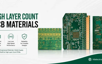
High Layer Count PCB Materials for Multilayer Boards
High layer count PCB materials guide for reliable multilayer manufacturing, covering core and prepreg selection, lamination yield, warpage, registration and lead time.
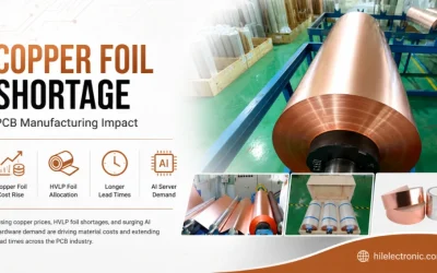
Copper Foil Shortage Impact on PCB Manufacturing
Copper foil shortage guide for PCB manufacturing, covering cost impact, HVLP foil, AI hardware demand, capacity pressure and supply risk management.
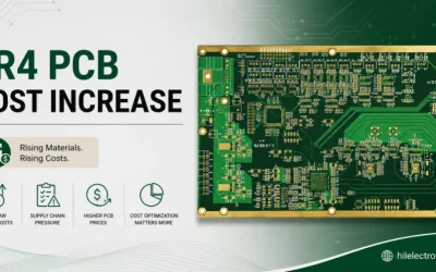
FR4 PCB Cost Increase for Electronics Manufacturers
FR4 PCB cost increase guide explaining raw material drivers, design decisions, reliability tradeoffs and ways to control cost without sacrificing quality.