
Back to blog
PCB Quality: The Definitive Guide to In-Circuit Testing (ICT)
.jpg "ICT(In-Circuit Testing)")
In-Circuit Testing (ICT) stands as a cornerstone in the PCB manufacturing industry, offering unparalleled insights into the functionality and integrity of electronic boards. This rigorous testing method is engineered to detect a wide array of potential issues, including solder shorts, open circuits, and component defects. Our commitment to excellence drives us to integrate advanced ICT methodologies, ensuring each PCB surpasses industry standards for performance and reliability.
ICT testing is pivotal for validating the electrical performance of printed circuit boards. By deploying sophisticated test probes, this process meticulously evaluates each component and solder joint, ensuring they meet predefined electrical parameters. The comprehensive nature of ICT allows for the identification and rectification of faults at the earliest stage, significantly reducing the time and cost associated with rework.
Key Benefits of ICT Testing
Unparalleled Quality Assurance
Comprehensive Component Verification: ICT testing scrutinizes every installed component for functionality, orientation, and value, confirming that each part is correctly placed and performing as expected. This thorough examination guarantees that the PCB operates flawlessly, meeting the desired specifications.
Solder Joint Inspection: Beyond component testing, ICT assesses solder joints, a critical aspect of PCB integrity. It identifies potential issues such as solder shorts and opens, which are pivotal for ensuring reliable electrical connections across the board.
Enhanced Manufacturing Efficiency
Early Defect Detection: By identifying defects at an early stage in the manufacturing process, ICT testing allows for immediate corrections, significantly reducing the need for rework or scrap. Early intervention streamlines production workflows, optimizing manufacturing timelines.
Reduced Rework Costs: The cost associated with reworking or scrapping defective boards can escalate quickly. ICT’s ability to pinpoint precise defects translates to targeted repairs, minimizing the expenditure on materials and labor while maximizing yield rates.
Elevated Product Reliability
Predictable Performance: ICT testing provides a high level of confidence in the PCB’s functionality, ensuring that the final product performs consistently in its intended application. This reliability is crucial for applications where failure can have significant implications, such as in medical devices or aerospace components.
Long-term Durability: By ensuring that only defect-free boards proceed to the next stages of production and ultimately into the field, ICT contributes to the long-term durability of the product. This reliability fosters trust among end-users and establishes a foundation for brand loyalty.
Competitive Advantage
Faster Time-to-Market: The efficiency gains from implementing ICT testing have a direct impact on production schedules, enabling faster time-to-market for new products. This speed can provide a competitive edge in fast-paced industries.
Compliance and Standards Adherence: ICT testing aids in compliance with international quality standards and regulations, an important factor for gaining access to and competing in global markets.
For production planning, it also helps to compare this topic with PCB electrical testing and PCB inspection and quality control before finalizing the fabrication or assembly package.

Advanced ICT Testing Techniques
Our approach to ICT testing incorporates a variety of advanced techniques, tailored to meet the specific requirements of each PCB project. These methodologies not only ensure accuracy but also adapt to the evolving landscape of electronic manufacturing.
Vectorless Test Techniques
Vectorless testing methods, such as the “Guardian” technique, offer a non-intrusive way to check for open circuits without the need for direct nodal access. This innovation is particularly beneficial for testing densely packed PCBs where traditional probing might be challenging.
Boundary Scan Testing
Boundary scan testing complements traditional ICT by examining integrated circuits that are inaccessible by physical test probes. This method is invaluable for testing complex digital circuits, further enhancing our testing capabilities.
Implementing ICT Testing: A Step-by-Step Overview
Step 1: Test Fixture and Program Development
Develop a custom ICT test fixture and program tailored to the specific PCB design. This involves mapping out all test points and determining the electrical tests to be performed.
Engineers use the PCB design files to identify test points for each component. They then design a test fixture that can physically contact these points and write a program that dictates the sequence of tests to be applied.
Step 2: Physical Setup
Securely place the PCB within the ICT test fixture, ensuring optimal contact with all test probes.
The PCB is carefully aligned and inserted into the test fixture. The fixture typically contains spring-loaded pins (test probes) that precisely align with the test points on the board, ensuring reliable electrical contact.
Step 3: Testing and Data Collection
Begin the ICT process, applying electrical signals to each test point and measuring the responses to identify any deviations from expected values.
The ICT machine activates, systematically applying signals to the test points as dictated by the test program. It records the electrical responses, such as resistance, capacitance, and voltage levels, comparing them against predefined criteria to identify discrepancies.
Step 4: Analysis and Correction
Analyze the collected data to pinpoint defects. Identified issues are corrected, and boards are retested to confirm the resolution of the defects.
Process:
Engineers review the test results, identifying any components or connections that failed the tests.
Faulty components are replaced or re-soldered as necessary. In some cases, design modifications may be recommended to address systemic issues.
Corrected boards are retested to ensure all previously identified issues have been resolved, confirming the board’s readiness for the next stages of production or assembly.

Related Articles
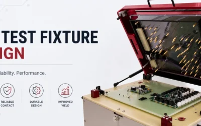
PCB Test Fixture Design: Bed-of-Nails, Flying Probe, and DFT
Compare PCB test fixture options, learn when bed-of-nails beats flying probe, and design test access for faster, repeatable production checks.
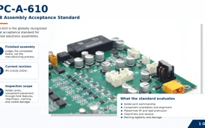
IPC-A-610 Standard for PCB Assembly Acceptance
Learn what IPC-A-610 covers for electronic assemblies, how Classes 1, 2, and 3 differ, and how buyers should specify assembly acceptance.
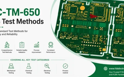
IPC-TM-650 PCB Test Methods Explained
Understand IPC-TM-650 PCB test methods, how the manual is organized, when to cite it, and how fabricators use tests for quality control.