
Back to blog
Optimizing PCB Design with Package-on-Package Technology

Package-on-Package(PoP )inspection
Package on Package (PoP) is an integrated circuit packaging method that vertically combines discrete logic and memory Ball Grid Array (BGA) packages. This technology addresses the electronics industry’s demands for fine pitch, smaller size, high signal processing speed, and smaller mounting real estate in products such as smartphones and digital cameras. PoP allows for electric connections between memory devices in the upper package and logic devices in the lower package, enabling independent testing and replacement of these components. These features reduce PCB assembly costs and complexity.
Package on Package (PoP) Structure
There are two widely used PoP structures: Standard PoP Structure and TMV PoP Structure.
Standard PoP Structure
In a standard PoP, logic devices are placed in the bottom package, featuring a fine pitch BGA solder to accommodate a large number of pin counts. The top package contains memory devices or stacked memories. To compensate for the insufficient pin counts in memory devices, a margin array can be applied at the margin of the two packages. Wire bonds are increasingly being replaced by flip chip technology in the bottom package to reduce package size, leading to a common 0.4mm solder pitch. The top package, containing dynamic random-access memory (DRAM) chips or DRAM chips with flash memory, requires finer solder pitches, now commonly at 0.4mm.
TMV PoP Structure
The Through Mold Vias (TMV) PoP is an improvement over the standard PoP, widely used in handheld electronic applications due to its fine pitch. Through mold vias in the bottom package and between the top solder in the bottom package and the solder in the top package provide electrical connections between the logic and memory devices. TMV PoP offers advantages such as shrinking package size, thickness, and warpage, while increasing interconnection density, performance, and reliability.
SMT Assembly Techniques of PoP
SMT plays a crucial role in the assembly of PoP components, offering two main techniques: pre-stacked PoP and on-board stacking PoP. These methods differ in their approach to stacking and soldering the PoP components onto the PCB.
- Pre-stacked PoP: This technique involves stacking the top and bottom packages of the PoP components before they are soldered to the PCB. The stacked components are soldered together first, creating a single pre-stacked device. This pre-stacked device is then attached to the surface of the PCB and undergoes reflow soldering to secure it in place. Pre-stacked PoP streamlines the assembly process by preparing the PoP components before mounting them onto the PCB, reducing the complexity of the soldering process.
- On-board stacking PoP: In contrast, on-board stacking PoP assembles the PoP components directly on the PCB. The bottom package is mounted onto the PCB first, followed by the top package, which is then either dipped in flux or solder paste before being placed onto the bottom package. The entire stack is then subjected to reflow soldering to create the final PoP assembly. On-board stacking PoP offers the advantage of assembling the PoP components directly on the PCB, allowing for more precise alignment and control during the soldering process.
Both techniques have their advantages and are used based on specific requirements and production capabilities. Pre-stacked PoP is often preferred for its simplicity and efficiency, while on-board stacking PoP offers more control over the assembly process and alignment of the PoP components.
Package-on-package (PoP) applications

SMT Procedure of PoP Components
- Solder Paste Printing of PoP Bottom Package: The solder paste printing process is determined by the component and pad sizes. Laser-cut and electroforming stencil templates are commonly used. Solder paste selection is based on printing clearance, with Type IV solder paste being increasingly used.
- PoP Top Package Dipping: The top package is dipped in either solder paste or flux. Proper dipping ensures the right amount of solder paste or flux is applied without causing soldering defects.
- PoP Component Positioning: Careful positioning of the top package is crucial to ensure accurate assembly and to withstand shock and vibration.
- Reflow Soldering of PoP: Lead-free soldering techniques are preferred for their reliability. Nitrogen with low oxygen content is used to reduce metal oxidation and ensure good wettability. Delicate reflow soldering temperature curves are necessary to prevent component or substrate deformation.
- Optical and X-ray Inspection of PoP: Various defects may occur during assembly and soldering, including open soldering, cold soldering, bridging, core ingression, and more. Inspection methods such as AOI, endoscopic inspection, and X-ray inspection are used to detect these defects.
The PoP assembly process requires precision, attention to detail, and adherence to quality standards to ensure reliable performance in electronic devices. Proper implementation of these procedures can lead to high-quality PoP assemblies with excellent performance and reliability.
Advantages of Package-on-Package (PoP)
Traditional flat arrangement of components on a PCB is being revolutionized by Package-on-Package (PoP) technology, which introduces a vertical stacking structure. This innovation significantly enhances PCB design by maximizing space utilization and enabling the integration of more functions into a smaller footprint, thus achieving higher performance in component combinations.
Space Efficiency and Enhanced Performance
The vertical stacking of components in a PoP configuration efficiently utilizes the limited space available on a PCB. This enables designers to incorporate more functions and features into their designs without increasing the overall size of the PCB. Additionally, the shorter vertical interconnections between the top and bottom packages optimize the distance between components. This reduction in trace length leads to lower resistance in the circuit, minimizing heat generation and signal delay, and enhancing the overall electrical performance of the circuit.
Modular Design and Easy Upgradability
One of the key advantages of PoP technology is its modular design, which allows memory components to be housed in separate packages. This modular approach makes it easier to upgrade or replace memory components without having to change the entire microcontroller or application processor. This flexibility not only simplifies the upgrade process but also reduces costs and downtime associated with replacing faulty components.
Individual Testing and Increased Reliability
The separation of memory components in PoP technology enables individual testing of different sections during the production process. This level of testing granularity ensures that each component meets the required specifications, leading to higher overall reliability of the final product. Additionally, the ability to test and replace individual components increases the longevity and upgradability of the device, further enhancing its overall reliability.
Design Flexibility and Compatibility
PoP technology offers designers greater flexibility in selecting memory packages that best suit their requirements. Designers can mix and match different microcontrollers and memory packages as long as they are compatible with the CPU package. This compatibility allows for a wide range of design options, enabling designers to tailor their designs to specific requirements and optimize performance.
Overall, Package-on-Package (PoP) technology offers a range of advantages, including space efficiency, enhanced performance, modular design, easy upgradability, individual testing, increased reliability, design flexibility, and compatibility. These advantages make PoP an attractive option for designers looking to maximize the functionality and performance of their PCB designs.
If this requirement affects sourcing or production release, compare it with circuit board components and high-current PCB fabrication before sending the final files for review.
Conclusion
The surface mount assembly of PoP components is a complex process that requires careful consideration of component structure, soldering techniques, and inspection methods. With the advancement of PoP technology, manufacturers can achieve higher integration densities, smaller form factors, and improved reliability in electronic devices.
PCB & PCBA quick quote
Related Articles

How to Clean Flux Off a PCB: The Right Method for Each Flux Type
Figure 1. How To Clean Flux Off Pcb reference image for PCB manufacturing review.Cleaning flux off a board sounds trivial until you use the wrong solvent on the wrong residue and end up with a hazy, corroded, or even more contaminated PCB. How to clean flux off a PCB...
PCB Potting Services: Compounds, Process, and Design Rules
Figure 1. PCB potting services image for Highleap Electronics PCB manufacturing and assembly review.PCB potting encases an assembled board (or a connector or module) in a solid block of resin, sealing it completely against moisture, vibration, chemicals, and...
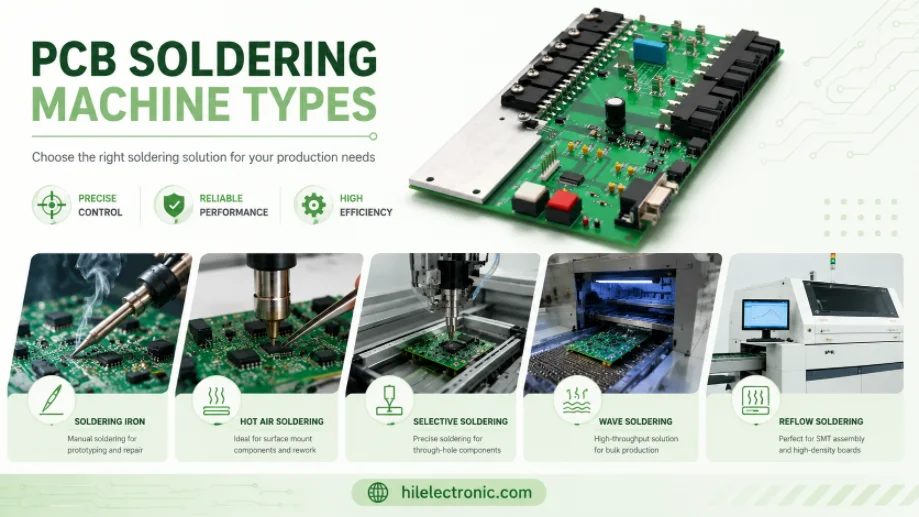
PCB Soldering Machine Types: Reflow, Wave, and Selective Equipment
Figure 1. PCB soldering machine types image for Highleap Electronics PCB manufacturing and assembly review.A PCB soldering machine is the production equipment used to join components to an assembly at scale, most often a reflow oven for SMT, a wave soldering system...
Take a Quick Quote