
AOI for PCB and PCBA Inspection in Manufacturing
")
In the rapidly evolving electronics manufacturing industry, precision and reliability are paramount, especially in the production of PCBs and PCB Assemblies (PCBAs). At Highleap Electronic, we are dedicated to delivering exceptional quality through advanced manufacturing processes, with Automated Optical Inspection (AOI) playing a pivotal role in achieving this goal. This article explores the critical importance of AOI in PCB and PCBA manufacturing, its operational principles, and how Highleap Electronic leverages AOI to ensure superior product quality and reliability.
Understanding AOI in PCB and PCBA Manufacturing
AOI is an advanced quality control technology used extensively in both PCB fabrication and PCB assembly. AOI employs high-resolution cameras and sophisticated image processing software to inspect the physical attributes of PCBs and PCBAs, identifying defects that may compromise functionality and reliability. This non-contact inspection method ensures that any issues are detected early in the manufacturing process, reducing the risk of costly rework and delays. From bare board to assembly inspection, see how Highleap Electronic ensures precision, detects defects, and reduces costs with cutting-edge AOI technology.
The Necessity of AOI Testing
Modern electronic devices are fundamentally dependent on PCBs, which serve as the backbone for electrical connections between components such as integrated circuits (ICs). From simple consumer electronics like watches and calculators to complex systems used in telecommunications, aerospace, and medical equipment, PCBs must meet stringent performance and reliability standards. The rapid advancement of technology and increasing demand for miniaturization and high-density designs have made AOI indispensable for ensuring flawless PCB and PCBA production.
Key Reasons for AOI Necessity:
-
- Complexity and Miniaturization: The shift to Surface Mount Technology (SMT) has led to smaller, more densely packed components, necessitating precise inspection to ensure correct placement and soldering.
- High Reliability Requirements: Industries such as telecommunications, aerospace, and medical devices require PCBs that perform reliably under demanding conditions.
- Cost Efficiency: Early detection of defects through AOI reduces the need for expensive rework and minimizes the risk of defective products reaching the market.
Core Attributes and Capabilities of AOI
At Highleap Electronic, AOI is integral to our quality assurance processes. Its key attributes ensure that both PCBs and PCBAs meet the highest standards of quality and performance:
This page focuses on how AOI is used inside PCB and PCBA manufacturing. For the basic definition of automated optical inspection, use what automated optical inspection means; for broader inspection records and process control, review PCB quality assurance process.
1. Comprehensive Defect Detection
AOI is capable of identifying a wide range of surface and assembly-related defects, including:
-
- Component Flaws: Missing parts, incorrect or misloaded components, shifted positions, incorrect orientation, and tombstoned parts.
- Solder Joint Issues: Insufficient or excessive solder, solder balls/splatter, solder bridging, and solder voiding.
- PCB Defects: Trace damage, hole plugging, foreign object debris, etching or plating issues, pad lifting, and marking flaws such as missing silkscreen prints or misaligned legends.
2. Versatility in Inspection Stages
AOI can be integrated at various stages of the manufacturing process:
-
- Bare PCB Inspection: Detects deviations in conductor traces, ensuring compliance with Gerber data, especially critical for high-frequency, high-power, and high-data transmission applications.
- PCBA Inspection: Verifies component placement, solder joint quality, and polarity, ensuring assembled boards function correctly.
3. Advanced Imaging and Algorithms
AOI systems utilize high-definition cameras and various lighting techniques (LED, infrared, ultraviolet) to capture detailed images of PCBs and PCBAs. Advanced algorithms, including template matching, object recognition, blob analysis, and vectoral imaging technology, process these images to identify defects with high accuracy and reliability.
4. Cost-Effective Quality Control
AOI offers a more affordable solution compared to other inspection methods like Automated X-ray Inspection (AXI), especially for common solder joint defects. This cost efficiency makes AOI a preferred choice for a wide range of applications.
5. Flexibility and Adaptability
AOI can be customized to meet specific customer needs, allowing it to be placed optimally within the manufacturing line to enhance inspection efficiency and reduce costs. For instance, placing AOI after the reflow soldering process allows immediate correction of any detected issues, preventing defective products from advancing further in production.
How AOI Works in PCB and PCBA Manufacturing
AOI operates by scanning the surface of a PCB or PCBA using high-resolution cameras. The captured images are then compared against predefined reference images or parameters using sophisticated image processing software. This comparison identifies any discrepancies, abnormalities, or errors, which are flagged for review.
Inspection Process
- Image Capture:
- Cameras: Color or black/white cameras mounted above the board.
- Lighting: Angled lighting to detect height variations and surface defects.
- Conveyance: Boards are conveyed under cameras for 100% coverage.
- Image Analysis:
- Software Comparison: Images are compared against a “golden board” reference.
- Defect Detection: Algorithms detect anomalies based on pixel differences, object shapes, and geometric features.
- Result Generation:
- Defect Reporting: Coordinates and size data of defects are recorded.
- Visual Evidence: Images or videos of detected flaws are generated.
- Pass/Fail Outcome: Boards are classified based on inspection results.
Advanced Inspection Algorithms
- Template Matching: Compares captured images pixel-by-pixel against a reference image.
- Object Recognition: Analyzes the shape and position of components to identify misplacements or incorrect parts.
- Blob Analysis: Groups similar pixels to inspect defects by separating objects from the background.
- Vectoral Imaging Technology: Uses geometric feature extraction to reduce false failures and improve inspection reliability.
Specialized AOI Testing at Highleap Electronic
Bare PCB AOI Testing
For bare PCBs, AOI verifies conductor trace images against Gerber data, identifying deviations such as narrowed yet unbroken traces. This is crucial for applications requiring high frequency, high power loads, high data transmission rates, and op-amps with high amplification factors and input resistances. In multilayer PCBs, AOI scans inner layers before they are pressed together, ensuring the high reliability of the final multilayer boards.
SMT AOI Testing
In Surface Mount Technology (SMT) PCB assembly, AOI plays a critical role in detecting defects early in the assembly process. Highleap Electronic employs both 2D and 3D AOI systems to ensure comprehensive inspection:
-
- 2D AOI: Cost-effective with single-angle image capture, suitable for detecting surface-level defects.
- 3D AOI: Provides multi-angle image capture and accurate height measurements, essential for detecting more complex defects and ensuring component integrity.
Defect Types Detected by SMT AOI:
-
- Component Flaws: Missing, misloaded, or incorrectly oriented parts.
- Solder Joint Issues: Insufficient or excessive solder, solder bridging, and voids.
- PCB Defects: Trace damage, hole plugging, and etching issues.
- Marking Flaws: Missing silkscreen prints and misaligned legends.

Reducing False Calls and Enhancing AOI Accuracy
False calls, where AOI incorrectly flags defects, can reduce manufacturing efficiency. Highleap Electronic employs several strategies to minimize false calls:
-
- Optimized Lighting and Thresholds: Fine-tuning lighting conditions and inspection thresholds to enhance defect detection accuracy.
- Enhanced Golden Board Reference: Incorporating all acceptable variations in the reference to prevent unnecessary rejection of valid boards.
- System Training: Training AOI systems with representative samples to improve defect classification.
- Regular Maintenance and Calibration: Ensuring AOI equipment remains accurate and reliable.
- Review and Feedback: Continuously reviewing AOI findings and adjusting inspection parameters based on historical data and defect patterns.
Implementing AOI Inspection Effectively at Highleap Electronic
To maximize the benefits of AOI, Highleap Electronic adopts a structured and strategic implementation process tailored to meet specific manufacturing requirements. We begin by selecting the most appropriate AOI technology based on the defect types and production needs of a particular project, ensuring our systems are optimized for both bare PCB and PCBA inspections. Inspection routines are then meticulously programmed to align with customer design specifications and global quality standards, guaranteeing precision and consistency across all inspected boards.
Recognizing the limitations of AOI, such as difficulties in detecting subsurface defects or shadowed areas, we complement it with other inspection methods like Automated X-ray Inspection (AXI) or In-Circuit Testing (ICT) when necessary. AOI inspection data is leveraged for focused repairs and root cause analysis, enabling our team to refine manufacturing parameters and prevent recurring defects. This data-driven approach not only improves product quality but also minimizes production downtime and waste.
Inline integration is another critical aspect of our AOI implementation. By embedding AOI directly within the production line, we can perform real-time defect detection and make immediate corrective adjustments to prevent errors from propagating further. To maintain accuracy and reliability, AOI programs and algorithms are continuously updated based on feedback and evolving manufacturing requirements. This commitment to ongoing improvement ensures that AOI remains a key contributor to Highleap Electronic’s high-quality PCB and PCBA production, supported by process controls such as first article inspection (FAI).
Why Highleap Electronic is Your Trusted AOI Partner
Choosing Highleap Electronic for your PCB and PCBA needs means partnering with a manufacturer that prioritizes quality, reliability, and customer satisfaction. Here’s why our AOI-driven approach sets us apart:
- Experience and Expertise: With extensive experience in PCB manufacturing and assembly, we understand the critical role of AOI in ensuring defect-free products.
- Advanced AOI Equipment: We utilize the latest AOI systems, including high-resolution cameras and vectoral imaging technology, to achieve unparalleled inspection accuracy.
- Comprehensive Services: From design optimization and rapid prototyping to large-scale production, our full-service approach ensures seamless project execution.
- Customer-Centric Approach: We work closely with our clients, tailoring AOI processes to meet specific requirements and ensuring your products meet all design and performance standards.
- Certified Quality Standards: Our ISO 9001:2015 certification and compliance with IPC-A-610 and J-STD-001 standards guarantee that our manufacturing processes and products adhere to global quality benchmarks.
As PCB designs continue to become more complex with smaller components and higher densities, the role of AOI will only increase in importance. Highleap Electronic remains committed to investing in the latest AOI technologies to meet the evolving needs of our customers. By combining innovation with a steadfast commitment to quality, we ensure that our clients receive reliable, high-performance PCBs and PCBAs every time.
Conclusion
AOI has become a standard inspection step in modern PCB and PCBA manufacturing, offering fast and repeatable detection of visible assembly defects. By identifying issues such as missing components, polarity/orientation errors, misalignment, and solder appearance anomalies at defined checkpoints, AOI helps improve process control, reduce rework, and support consistent production quality. At Highleap Electronic, AOI is applied according to project requirements and inspection criteria across appropriate stages of the manufacturing flow, and can be combined with other inspection or electrical test methods when additional coverage is required for specific designs, packages, or reliability targets.
Get a Free PCB & PCBA Quote

Recommended Posts

IPC-A-610 Standard for PCB Assembly Acceptance
Figure 1. IPC-A-610 PCB assembly acceptance standard...

IPC-TM-650 PCB Test Methods Explained
Figure 1. IPC-TM-650 PCB test methods IPC-TM-650 is IPC's...
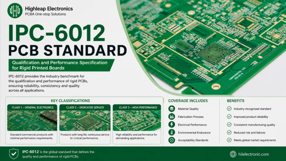
IPC-6012 Standard for Rigid PCB Fabrication
Figure 1. IPC-6012 standard for rigid PCB fabrication...

Electrical Testing PCB Flying Probe vs ICT vs FCT
Figure 1. Comparison of Electrical Testing PCB methods:...
How to get a quote for PCBs
Let us run DFM/DFA analysis for you and get back to you with a report.
You can upload your files securely through our website.
We require the following information in order to give you a quote:
-
- Gerber, ODB++, or .pcb, spec.
- BOM list if you require assembly
- Quantity
- Turn time
In addition to PCB manufacturing, we offer a comprehensive range of electronic services, including PCB design, PCBA (Printed Circuit Board Assembly), and turnkey solutions. Whether you need help with prototyping, design verification, component sourcing, or mass production, we provide end-to-end support to ensure your project’s success. For PCBA services, please provide your BOM (Bill of Materials) and any specific assembly instructions. We also offer DFM/DFA analysis to optimize your designs for manufacturability and assembly, ensuring a smooth production process.