
Advanced PCB Manufacturing for HDI Solutions (High-Density Interconnect)

Electronic devices are becoming increasingly powerful while shrinking in size, making the design of their circuit boards more challenging. Standard PCBs can’t meet the needs of modern systems that require dense wiring, specialized materials, and high-precision manufacturing. Whether for telecom equipment, aerospace systems, self-driving cars, or advanced medical devices, you need PCBs that effectively manage signals, heat, and stress under demanding conditions.
At Highleap Electronic, we specialize in producing advanced HDI PCBs that go beyond the capabilities of traditional board technologies. Our boards use high-performance materials such as ceramic substrates, metal-based boards, and glass—ensuring your project gets the precision and durability it requires. We provide robust, production-ready solutions that address the unique needs of complex electronic devices.
Our expertise in HDI PCB manufacturing includes handling multiple lamination cycles, creating ultra-fine traces, and ensuring precise impedance control. With state-of-the-art equipment and extensive engineering know-how, we are equipped to tackle the most challenging projects. Our comprehensive HDI solutions ensure the highest levels of performance and reliability, helping your next-generation systems excel.
Advanced HDI PCB Solutions for Complex and Specialized Manufacturing
If you’re looking for a manufacturer capable of delivering advanced HDI PCB solutions for complex and high-difficulty designs, or if you need precision PCB prototyping, batch production, and assembly, Highleap Electronic is your ideal partner. We specialize in providing custom PCB solutions that meet the rigorous demands of engineers, R&D professionals, and procurement managers in the electronics industry. Our services include:
-
- Exotic Substrates and Mixed Constructions: We offer PCB solutions designed for extreme conditions, such as ceramic PCBs for stable RF signal transmission, metal-core designs for superior heat dissipation, and glass substrates for ultra-high-frequency and optical interconnections. These advanced configurations are part of our broader HDI solutions for extreme environments and next-gen applications.
- High Layer Counts and Tight Tolerances: We can manufacture advanced HDI PCBs with up to 60 layers, with trace/space down to 2/2 mil, enabling miniaturization, enhanced signal integrity, and exceptional functional density.
- Meticulous Precision in Drilling and Plating: Our laser-drilled microvias, strict annular ring control, and optimized aspect ratios ensure robust interconnections and stable impedance across all designs.
- Controlled Impedance Across Complex Stack-Ups: We excel in multi-layer stack-up designs, combining different dielectric materials while maintaining stringent impedance tolerances, ensuring predictable signal performance and reliability.
Whether you’re working on prototypes, small-batch production, or large-scale manufacturing and assembly, Highleap Electronic offers comprehensive support from design to final product, helping you achieve technical excellence with advanced HDI PCBs that meet the highest standards in manufacturing and performance.
Advanced PCB Materials and Their Impact on Performance
As electronics continue to evolve, so do the materials used to build PCBs. At Highleap Electronic, we excel in fabricating boards that extend well beyond standard FR4 and high-Tg laminates, leveraging advanced materials to meet stringent requirements:
-
- Metal Core PCBs (Aluminum, Copper):
Ideal for high-power LEDs, automotive drives, and industrial converters. Metal core boards dissipate heat efficiently, maintain structural rigidity, and support heavy copper (up to 10oz) for high current applications. - Ceramic Substrate PCBs (Alumina, Aluminum Nitride):
Perfect for aerospace, microwave modules, and RF communication systems. Ceramic substrates offer excellent thermal conductivity, dimensional stability, and low dielectric losses, ensuring consistent performance under demanding conditions. - Glass PCBs:
Near-perfect dimensional stability and exceptional electrical properties make glass-based substrates suitable for ultra-high-frequency digital circuits, photonics, optical interconnects, and next-generation communication systems. - PTFE-Based and Low-Dk Laminates (e.g., Rogers, Taconic):
For high-speed digital and RF applications, PTFE and specialized low-Dk laminates reduce signal attenuation and ensure stable impedance, enabling high-frequency devices and ultra-fast data transfer. These materials are essential in HDI solutions aimed at high-frequency, low-loss designs. - Polyimide, Flexible, and Rigid-Flex Boards:
Polyimide-based flexible circuits and rigid-flex combinations offer enhanced durability, reduced connector counts, and dynamic bending capabilities, essential for aerospace, wearables, and miniaturized consumer electronics. - Mixed-Dielectric Stack-Ups (Hybrid PCBs):
Combining diverse materials within one board allows engineers to optimize dielectric properties, mechanical strength, and thermal behavior. This approach is ideal for balancing multiple performance requirements in a single design. This approach is frequently used in advanced HDI PCBs, where performance needs vary across different zones of the same circuit.
- Metal Core PCBs (Aluminum, Copper):
Highleap provides PCB manufacturing and assembly with advanced HDI PCB solutions, impedance control, and cutting-edge materials for aerospace, telecom, and medical sectors. From advanced HDI PCBs using mixed-dielectric stack-ups to HDI solutions that demand stable impedance in high-frequency systems, our team ensures every design is optimized for performance, reliability, and manufacturability.
High-Density Interconnect (HDI) and Multi-Lamination Expertise
Creating boards that push technical limits demands meticulous HDI solutions and multiple lamination cycles. At Highleap Electronic, we craft advanced HDI PCBs up to 60 layers, achieving inner and outer layer trace/space as fine as 2/2 mil, ensuring exceptional routing density and compact form factors. We also support mechanical drilling and laser drilling with the following specs:
- Minimum Mechanical Drilling/Annular Ring: 0.15mm/0.127mm, enabling stable plated through-holes with excellent copper plating distribution and reliable interconnections.
- Minimum Laser Drilling/Annular Ring: 0.075mm/0.075mm, supporting stacked, staggered, and filled microvia structures that are essential in advanced HDI designs.
Aspect ratios are a critical measure of drill depth versus hole diameter. Highleap Electronic maintains up to 20:1 aspect ratio for mechanical drilling and 1:1 for laser drilling, ensuring robust via reliability even in thick, multilayer constructions.
Complex HDI boards often require multiple sequential laminations. Throughout this process, we control board thickness from 0.4mm to 8mm, adhere to a board thickness tolerance of ±0.1mm for <1.0mm thickness and ±10% for ≥1.0mm thickness, ensuring stable dimensions essential for predictable impedance and mechanical consistency—key factors in delivering reliable HDI solutions for demanding applications.

Dimensional Stability, Impedance Control, and Finishing Options
As signal frequencies climb and margins shrink, controlling impedance variation is paramount in delivering reliable HDI solutions. Highleap Electronic’s impedance tolerance capabilities are critical to the performance of advanced HDI PCBs, with:
- Single-Ended: ±5Ω (≤50Ω), ±7% (>50Ω)
- Differential: ±5Ω (≤50Ω), ±7% (>50Ω)
Our manufacturing precision extends to every detail:
- Min Board Size: 10*10mm for ultra-compact devices
- Max Board Size: 22.5*30inch for large-scale systems
- Contour Tolerance: ±0.1mm for high-precision panelization and complex board outlines
For advanced component packaging, we accommodate BGA pitches down to 7mil and SMT pads at 7*10mil, supporting the latest high-pin-count, fine-pitch components on advanced HDI PCBs.
Surface treatment options are equally diverse. We offer ENIG, immersion silver, immersion tin, HASL, OSP, ENEPIG, flash gold, hard gold plating, and selective gold finger finishes. Multiple solder mask colors (green, black, blue, red, matte green) and legend options (white, black, red, yellow) allow for product differentiation and functional marking. The minimum solder mask clearance is 1.5mil and solder mask dam is 3mil, ensuring precise coverage and minimized solder bridging.
Quality Assurance and Reliability
In advanced HDI PCBs, maintaining tight tolerances and complex structures wouldn’t matter if reliability suffered. To ensure consistent reliability across our HDI solutions, Highleap Electronic integrates rigorous quality controls at every stage:
-
- PTH/NPTH Tolerances: ±0.075mm for plated through holes and ±0.05mm for non-plated holes, supporting stable component mounting and signal integrity.
- Press Fit Hole Tolerance: ±0.05mm ensures reliable mechanical press-fit component assembly.
- Countersink Tolerance: ±0.15mm provides stable mechanical interfaces and secure component seating.
- Bow & Twist: ≤0.3% ensures boards remain flat and stable, a crucial factor in automated assembly and long-term reliability.
By leveraging Automated Optical Inspection (AOI), X-ray imaging for via and plating integrity, and various electrical and environmental stress tests, we guarantee that each board—including the most demanding advanced HDI PCBs—meets or exceeds industry standards and your project requirements.

DFM Support and End-to-End Solutions with Advanced HDI Expertise
When designing for cutting-edge HDI solutions, engineers face unique challenges due to complex material requirements, multi-layer stack-ups, and precise impedance control. At Highleap Electronic, we specialize in guiding you through the entire process with our comprehensive design-for-manufacturability (DFM) support. From the very beginning of your project, our team helps identify optimal material combinations, advanced stack-up configurations, and precise drilling strategies tailored to your advanced HDI PCB needs, ensuring streamlined production and high-quality outcomes.
Our DFM guidance reduces the risk of costly redesigns and accelerates your time-to-market by proactively addressing potential challenges. Whether you’re working on multi-layer HDI boards, fine-line routing, or specialized substrates, we ensure that every detail is optimized for manufacturability and performance.
In addition to PCB fabrication, we provide a complete suite of services, including PCB assembly and thorough testing. Our integrated approach covers every phase of the project—from sourcing high-quality components to functional validation of your HDI solutions—ensuring that the final product meets your exact specifications and quality standards. With Highleap Electronic as your partner, you benefit from expertise in advanced HDI PCB design and manufacturing, all while maintaining control over cost and schedule.
Partnering with Highleap Electronic for Your Next Breakthrough
When your designs demand extraordinary capability—60-layer stack-ups, 2/2 mil trace/space, 10oz copper on both inner and outer layers, or specialized substrates like metal, ceramic, and glass—Highleap Electronic is ready to deliver. Our flexible approach supports everything from quick-turn prototypes to full-scale production, adapting to your project’s evolving requirements.
Engineers, innovators, and sourcing professionals who require precision Electronics PCB Manufacturing will find a strategic ally in Highleap Electronic. We understand that complex designs, extreme materials, and demanding tolerances aren’t just technical challenges—they’re opportunities to achieve unprecedented performance and reliability.
Contact Highleap Electronic Today
If you are ready to move beyond standard PCBs and explore the capabilities that state-of-the-art HDI, multi-lamination, and exotic material solutions can provide, contact Highleap Electronic. Our team of experts is prepared to guide you through material selection, stack-up optimization, and every meticulous manufacturing detail to bring your vision to reality.
In a world where technical limits are constantly being pushed, let us help you transcend boundaries and create PCBs that define the cutting edge of electronic innovation.

Recommended Posts

Outdoor Lighting PCB Manufacturing & Assembly by Highleap Electronics
Figure 1. outdoor lighting PCB production and assembly...

Lighting PCB Manufacturer: PCB Fabrication, PCB Assembly & Turnkey LED Lighting
Figure 1. Lighting PCB manufacturer overview for LED light...

Audio DSP: How It Works, What It Does, and How the PCB Behind It Gets Built
On this page What Audio DSP Actually Does Core Audio DSP...
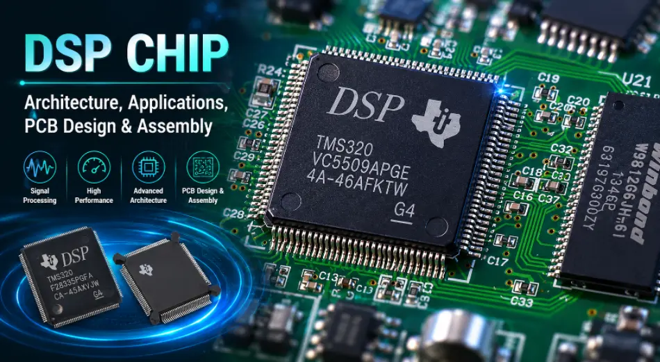
DSP Chip PCB Design and Assembly Guide
High-performance DSP chip boards need design, fabrication,...
How to get a quote for PCBs
Let us run DFM/DFA analysis for you and get back to you with a report.
You can upload your files securely through our website.
We require the following information in order to give you a quote:
-
- Gerber, ODB++, or .pcb, spec.
- BOM list if you require assembly
- Quantity
- Turn time
In addition to PCB manufacturing, we offer a comprehensive range of electronic services, including PCB design, PCBA (Printed Circuit Board Assembly), and turnkey solutions. Whether you need help with prototyping, design verification, component sourcing, or mass production, we provide end-to-end support to ensure your project’s success. For PCBA services, please provide your BOM (Bill of Materials) and any specific assembly instructions. We also offer DFM/DFA analysis to optimize your designs for manufacturability and assembly, ensuring a smooth production process.