
What Are HDI Circuit Boards? Benefits, Uses, and How Highleap Builds Them

In the rapidly advancing field of electronics, HDI circuit boards (High-Density Interconnect boards) have become essential for building powerful, compact, and high-performance devices. HDI PCBs, or high-density interconnect PCBs, are widely used in smartphones, wearables, automotive electronics, and medical equipment. Their ability to support complex HDI PCB designs and space-efficient layouts makes them ideal for next-generation electronics.
As HDI PCB manufacturing continues to evolve, these boards enable engineers to achieve high functionality within smaller footprints. This article explores HDI circuit board technology in depth, covering design principles, fabrication techniques, and related solutions such as microvia PCBs and HDI flex PCBs.
What is an HDI Circuit Board?
An HDI circuit board is a type of printed circuit board (PCB) designed to provide a higher wiring density per unit area compared to conventional PCBs. By integrating microvias, HDI circuit boards facilitate denser component layouts, greater signal integrity, and reduced interference, all while allowing for highly compact designs. These characteristics make HDI PCBs particularly suitable for devices requiring high performance in small form factors.
Key Features of HDI Circuit Boards
HDI PCBs are recognized for their use of microvias, blind vias, and buried vias. Microvias are tiny holes that enable direct connections between specific layers within the board, making HDI technology highly efficient for layered designs and high-density layouts. Additional features that distinguish HDI PCBs include:
- High-Density Interconnections: HDI PCBs allow for higher wiring density, resulting in maximized functionality in minimal space.
- Multilayer Structure: These boards frequently contain multiple layers, allowing for complex routing.
- Improved Signal Integrity: Shorter connections and minimized signal paths enhance signal clarity, essential in high-speed applications.
Understanding HDI PCB Levels: 1-N-1, 2-N-2, and Beyond
HDI PCBs are often classified by their levels or layer counts, which represent the number of microvia layers and interconnects. Levels start at 1-N-1 (one layer of microvias on each side of the core) and extend to any-layer HDI, where all layers are interconnected, allowing maximum component density. Each HDI level offers a progressively complex and highly functional design option. Here’s a breakdown:
- 1-N-1 HDI PCB: The basic level of HDI with a single microvia layer on each side of the core, suitable for simpler designs with moderate component density.
- 2-N-2 HDI PCB: Incorporates two microvia layers on each side, ideal for more complex designs that need greater interconnect density.
- Any-Layer HDI PCB: In this advanced type, all layers are interconnected, providing unmatched density and versatility. Often used in high-performance applications such as 5G and advanced computing.
These HDI levels guide designers in choosing the most appropriate board complexity for their application requirements, available space, and budget constraints.
Benefits of HDI Circuit Boards
HDI circuit boards are advantageous in various applications due to their compact design and high performance. Here are some of the primary benefits:
- Reduced Size and Weight: HDI PCBs support high-density component placement in a smaller footprint, making them ideal for modern, compact electronic devices like smartphones, wearables, and tablets.
- Increased Functionality: HDI PCB design allows more components to be included within a smaller area, increasing functionality without expanding the physical size of the board.
- Enhanced Signal Integrity: The close placement of components and shorter interconnects reduce electrical noise, enhancing signal integrity. This is particularly important for high-speed and high-frequency applications.
- Higher Reliability: With fewer traditional vias and the use of microvias, HDI boards generally have higher mechanical reliability and are less prone to failure from thermal and mechanical stress.

HDI Circuit Boards Manufacturing Services
Applications of HDI Circuit Boards: Rapid Manufacturing for Diverse Sectors
HDI circuit boards have become essential across various industries due to their compact size, high performance, and reliability. At the forefront of electronics innovation, HDI circuit boards are integral to industries where miniaturization and functionality are paramount, such as consumer electronics, automotive systems, medical devices, and aerospace.
Given the advancements in manufacturing techniques, many of these HDI PCB types can be produced quickly and efficiently, allowing for faster time-to-market and reducing development cycles. Below, we explore their applications and how our rapid manufacturing capabilities make HDI boards accessible across sectors.
Consumer Electronics
The demand for compact, powerful devices drives much of the innovation in HDI circuit board technology. HDI boards enable the production of high-density, small form-factor devices, making them ideal for smartphones, tablets, laptops, and wearables. The compact design of HDI PCBs is achieved through microvia and multilayer stacking technologies, allowing for high functionality within minimal space.
Our advanced manufacturing facilities allow us to produce HDI circuit boards quickly and at scale for consumer electronics manufacturers. Through the use of automated processes, such as high-speed laser drilling for microvias and rapid sequential lamination, we reduce production time significantly. This speed is crucial in the fast-paced consumer electronics industry, where time-to-market can determine success.
Automotive Electronics
In the automotive sector, HDI PCBs are used in applications that demand durability and compact design. From advanced driver-assistance systems (ADAS) to infotainment systems and sensor modules, HDI PCBs support the growing complexity of modern vehicles. These boards enable high-speed data processing and power distribution within the limited space available in automotive components.
We are equipped to rapidly manufacture these automotive-grade HDI PCBs, meeting industry standards for durability and reliability. Our quick turnaround times help automotive manufacturers develop, test, and implement new technologies more efficiently. By streamlining the production process, we help automotive OEMs bring cutting-edge, HDI-based systems to market faster, while ensuring the boards withstand the harsh conditions typical of automotive applications.
Medical Devices
The medical industry increasingly relies on HDI circuit boards due to their ability to support high-precision, compact, and reliable designs. Medical applications—such as imaging systems, diagnostic devices, and wearable health monitors—demand HDI PCBs that are not only compact but also highly reliable and capable of handling sensitive data accurately.
We offer expedited manufacturing of HDI PCBs tailored for medical applications. Our manufacturing process ensures strict quality control and adherence to medical-grade standards, allowing us to produce HDI boards that meet the stringent requirements of the healthcare industry. By minimizing production lead times, we enable medical device manufacturers to move quickly from prototyping to full-scale production, helping new medical technologies reach healthcare providers faster.
Aerospace and Defense
Aerospace and defense applications require robust, high-performance HDI PCBs that can operate reliably under extreme conditions. HDI boards are essential for navigation systems, avionics, missile systems, and communication devices, where durability, miniaturization, and high-density interconnects are crucial.
Our manufacturing facilities are designed to meet the rigorous demands of the aerospace and defense sectors. Through specialized testing and advanced fabrication processes, we ensure that each HDI PCB meets the high reliability and performance standards required in these fields. The streamlined production process allows us to fulfill urgent orders efficiently, ensuring rapid deployment of mission-critical technologies.
Our Capabilities for Rapid HDI PCB Manufacturing
Our specialized facilities and advanced technology allow us to produce HDI circuit boards quickly and accurately across a wide range of applications. We leverage the following capabilities to support rapid HDI PCB manufacturing:
- High-Speed Laser Drilling for Microvias: Precision laser drilling enables us to produce microvias essential for HDI PCB designs at a rapid pace, maintaining accuracy and reliability.
- Automated Sequential Lamination: By automating the lamination process, we create multi-layered HDI boards with minimal turnaround time, ensuring layer alignment and quality.
- Efficient Testing Protocols: We use advanced testing methods, such as automated optical inspection (AOI) and flying probe testing, to ensure each HDI board meets specifications before shipping. This minimizes production time without compromising quality.
- Flexible Production Volumes: Our manufacturing processes are adaptable to both small prototype runs and large-scale production, enabling us to meet the varied needs of our clients across different industries.
- Material Sourcing and Inventory Management: We maintain an efficient supply chain for high-quality materials, ensuring uninterrupted production even under tight deadlines.
Microvias in HDI PCB Technology
Microvias are small-diameter vias that provide interconnects between layers in an HDI board. There are three main types of microvias used in HDI PCB design:
- Blind Vias: These connect an outer layer with an inner layer but do not extend through the entire PCB. Blind vias are beneficial for creating interconnects without occupying valuable board space on the outer layers.
- Buried Vias: Buried vias connect two inner layers and are entirely enclosed within the board. They do not extend to the outer layers, allowing designers to maximize surface area for component placement.
- Stacked Vias: Stacked vias are microvias placed on top of each other to create a vertical interconnect path. Stacked vias are beneficial in high-layer-count boards, where traditional via structures would require more space.
HDI circuit boards are a cornerstone in multiple industries, from consumer electronics to aerospace. Our rapid manufacturing capabilities for HDI PCBs empower companies to innovate, test, and deploy new technologies faster than ever before. With high-speed production, rigorous testing, and flexible volumes, we provide our clients the edge they need to stay competitive in fast-evolving markets.
Whether for a new wearable device, an advanced automotive sensor, or a mission-critical aerospace system, our HDI circuit boards are manufactured to meet the most demanding standards, and they’re delivered on time to fuel your next innovation.

Challenges in HDI Circuit Board Manufacturing
Precision Requirements and Tight Tolerances
The manufacturing of HDI circuit boards involves advanced processes and precise techniques, making it both intricate and costly. High-precision requirements are a particular challenge; the tiny, densely packed microvias and narrow trace widths essential to HDI circuit board design demand exceptional accuracy.
Even minor deviations during fabrication can impact board performance, necessitating stringent quality control and highly specialized equipment. This precision also means that HDI circuit boards have a lower margin for error compared to traditional PCBs, which can increase manufacturing complexity.
Thermal and Mechanical Stress Management
Thermal and mechanical stress management is another critical area. The compact, high-density layout of HDI circuit boards can lead to significant heat buildup during operation. Effective thermal management strategies must be integrated into the design to prevent overheating, especially in boards with multiple layers or high-power components.
Furthermore, the structure of microvias, while ideal for space-saving, is more vulnerable to thermal cycling and stress over time. Manufacturers must test extensively to ensure these boards withstand the mechanical stresses they may encounter in real-world applications.
Material Selection and Production Costs
Lastly, material selection and fabrication costs add to the complexity. Producing HDI circuit boards often requires premium materials that are both durable and compatible with the advanced manufacturing processes, such as sequential lamination and laser drilling. This drives up the cost of production, making HDI circuit boards more expensive than conventional PCBs.
As the demand for compact, high-performance electronics grows, manufacturers continue to innovate to make HDI circuit board production more efficient while managing these technical and cost-related challenges.
Conclusion
HDI circuit boards represent a transformative advancement in PCB technology, providing designers with the capability to develop compact, high-performance, and highly reliable solutions that meet the demands of modern applications. Leveraging our expertise in HDI PCB technology, we enable you to harness the benefits of microvias, sophisticated interconnect techniques, and multilayer constructions, achieving levels of performance and miniaturization that redefine possibilities in electronic design.
As technology advances, HDI PCBs continue to drive innovation across industries, facilitating the development of ever-smaller, faster, and more powerful devices. By partnering with us, you gain access to a leader in HDI PCB design and fabrication—ensuring that your products are built to excel in even the most demanding environments. Our commitment to precision, quality, and innovation ensures that your HDI circuit boards are manufactured to meet the highest standards, giving your team a competitive edge in delivering next-generation solutions to market.
FAQs
1. What are the technical advantages of HDI Circuit Boards?
- HDI Circuit Boards offer superior signal integrity, faster data transmission, and smaller form factors compared to traditional PCBs. These advantages are achieved through advanced interconnect technologies like microvias and multilayer constructions, making them ideal for high-performance electronic devices.
2. What are the best design practices for HDI PCBs?
- Designing HDI PCBs requires careful consideration of layout strategies that optimize space and connectivity. Key practices include maximizing the use of microvias, managing layer stacking for efficient routing, and ensuring compliance with HDI design rules to maintain reliability and performance.
3. What are the main manufacturing challenges associated with HDI PCBs?
- Manufacturing HDI PCBs involves complex processes such as laser drilling and sequential lamination, which can increase production costs. Understanding these challenges helps in evaluating manufacturing feasibility and exploring cost-effective solutions without compromising quality.
4. In which applications are HDI PCBs most suitable?
- HDI PCBs are well-suited for industries requiring compact, high-performance solutions, including consumer electronics, automotive systems, aerospace, and medical devices. Their ability to handle high-density interconnections and stringent performance requirements makes them indispensable in modern electronic designs.
5. How do I choose a reliable supplier for HDI PCBs?
- When selecting a supplier, consider their certifications (such as ISO, UL) and expertise in HDI PCB manufacturing. Look for suppliers with a proven track record in delivering high-quality products and providing comprehensive technical support, ensuring reliable performance and successful project outcomes.

Recommended Posts

RF Transceiver PCB Manufacturing and Assembly
Table of contentsRF Transceiver PCB Manufacturing and...
RFSoC Board PCB Manufacturing and Assembly One-Stop Service
Highleap Electronics supports customer-designed RFSOC...
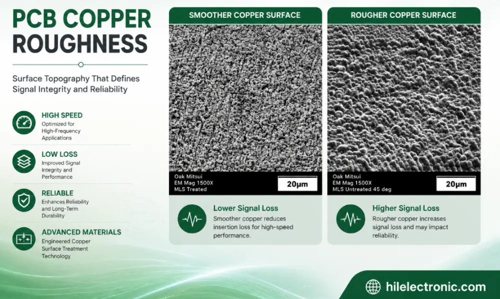
PCB Copper Roughness: Signal Loss, Material Selection and Manufacturing Control
Table of contentsWhat Is PCB Copper Roughness?How Copper...
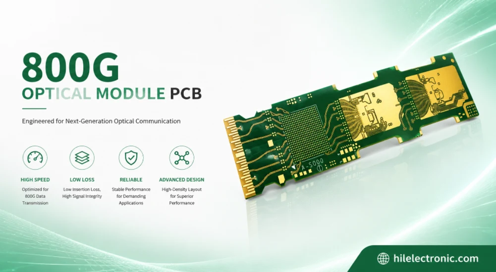
800G Optical Module PCB Manufacturing and Assembly Service
Table of contentsWhat Makes an 800G Optical Module PCB...
How to get a quote for PCBs
Let us run DFM/DFA analysis for you and get back to you with a report.
You can upload your files securely through our website.
We require the following information in order to give you a quote:
-
- Gerber, ODB++, or .pcb, spec.
- BOM list if you require assembly
- Quantity
- Turn time
In addition to PCB manufacturing, we offer a comprehensive range of electronic services, including PCB design, PCBA (Printed Circuit Board Assembly), and turnkey solutions. Whether you need help with prototyping, design verification, component sourcing, or mass production, we provide end-to-end support to ensure your project’s success. For PCBA services, please provide your BOM (Bill of Materials) and any specific assembly instructions. We also offer DFM/DFA analysis to optimize your designs for manufacturability and assembly, ensuring a smooth production process.