
AI Server PCB Materials: Low-Loss Laminates, Stack-Up, Thermal and PCBA Guide
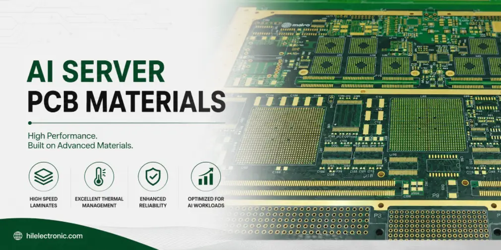
Choosing AI server PCB materials is not the same as choosing a normal FR-4 laminate. AI server hardware combines high-speed SerDes channels, GPU or accelerator power delivery, high layer count, dense BGA routing, heavy copper planes, strict impedance control and long-term thermal reliability in one board system. If the wrong PCB material is selected, the problem may appear as insertion loss, closed eye diagrams, unstable impedance, excessive temperature rise, via fatigue, CAF risk, warpage, assembly defects or delayed production because the required laminate is unavailable.
This guide is written for engineers, hardware startups, procurement teams and product managers who are searching for practical answers to questions such as: What PCB material should I use for an AI server board? Is FR-4 enough? When do I need Megtron, Tachyon, Astra, specialty low-loss laminate or another low-loss laminate? How do Dk, Df, copper roughness and glass weave affect 112G or 224G channels? What should I ask a PCB manufacturer before freezing the stack-up?
Highleap Electronics is a PCB manufacturing and PCB assembly factory. For AI server, GPU, accelerator, networking and high-performance computing projects, the correct approach is not to select a material name in isolation. The material must be checked together with the signal speed, channel length, layer count, impedance structure, copper weight, via structure, lamination process, soldering profile and component package requirements.
Quick answer: AI server PCBs usually need a mix of very-low-loss or ultra-low-loss laminates for high-speed layers, low-profile or HVLP copper foil for reduced conductor loss, spread-glass or low-Dk glass styles for skew control, high-Tg and low-CTE materials for reliability, and carefully planned hybrid stack-ups to balance performance and cost. Standard FR-4 may still be used for low-speed, control or power-only sections, but it is usually not suitable for long 112G/224G SerDes paths.
What AI Server PCB Materials Need to Solve
AI servers place unusual stress on PCB materials because the board is not only a mechanical carrier for components. It is part of the electrical channel, the power delivery network, the heat path and the reliability structure. The material directly affects signal loss, impedance stability, timing skew, thermal expansion, soldering survivability and final production yield.
A conventional industrial PCB may be selected mainly by Tg, copper weight, board thickness and cost. An AI server PCB needs a much deeper review. The material must support high-speed digital communication between GPUs, CPUs, memory devices, retimers, switches, NICs, backplanes, storage controllers and power modules. The board may contain dozens of layers, multiple lamination cycles, blind and buried vias, back-drilling, very dense BGA escape routing and large current paths.
| AI server requirement | Material impact | What to check before fabrication |
|---|---|---|
| 112G / 224G / high-speed SerDes | Requires low Df, stable Dk, smooth copper and controlled glass weave | Insertion loss target, trace length, impedance, copper foil type, laminate data at relevant frequency |
| GPU and accelerator power demand | Needs heavy copper planes, low DC resistance and thermal reliability | Copper weight, plane structure, via current capacity, thermal path, assembly temperature profile |
| High layer count | Increases lamination difficulty, registration risk and via reliability stress | Lamination cycle, material CTE, resin flow, drill quality, stack-up balance |
| Fine-pitch BGA routing | Often requires HDI, microvias, thin dielectrics and good dimensional stability | BGA pitch, via-in-pad need, microvia reliability, solder mask registration, PCBA process window |
| Long operating life in data centers | Requires high thermal stability, low moisture absorption and CAF resistance | Tg, Td, T288, Z-axis CTE, CAF test history, reflow compatibility |
The most important point is that the “best” AI server PCB material depends on the board function. A GPU baseboard, accelerator card, switch board, backplane, storage controller and power distribution board do not always need the same laminate. Using ultra-low-loss material everywhere may increase cost unnecessarily. Using standard FR-4 on critical high-speed layers may cause electrical failure. A good material plan separates critical layers from non-critical layers and builds a stack-up that satisfies both engineering and production requirements.
Material Requirements for Different AI Server Boards
An AI server contains several PCB types. Each board has a different balance of signal integrity, power delivery, thermal load and cost sensitivity. Before choosing a laminate, identify the board type and the interfaces it carries.
| Board type | Main challenge | Typical material direction |
|---|---|---|
| GPU / accelerator board | High-speed GPU interconnect, HBM-related routing environment, dense BGA escape, high current | Very-low-loss or ultra-low-loss laminate on high-speed layers; high-Tg, low-CTE core/prepreg; HVLP copper; HDI-compatible material |
| AI server motherboard | CPU, GPU, memory, PCIe, management, power and multiple connector zones | Hybrid stack-up: low-loss material for critical SerDes layers, lower-cost high-Tg material for control and power areas where allowed |
| High-speed switch PCB | Many long high-speed channels, tight loss budget, connector and via discontinuities | Ultra-low-loss laminate, very smooth copper, strict impedance control, back-drill-friendly stack-up |
| Backplane / midplane | Long reach channels, connector transitions, thick board, via stub control | Low-loss or ultra-low-loss laminate across signal layers; controlled CTE; strong drilling and back-drilling process capability |
| NIC / networking card | High-speed Ethernet, optical module interface, retimer placement, thermal density | Low-loss laminate for high-speed paths; stable Dk for impedance; selective high-performance material for critical zones |
| Power distribution board | High current, voltage drop, heat, mechanical strength | High-Tg FR-4 or high-reliability laminate with heavy copper; material selection focuses more on thermal and mechanical reliability than ultra-low signal loss |
This is why a search for “AI server PCB materials” cannot be answered by one material name. The right answer starts with the signal map. Which layers carry 112G or 224G differential pairs? Which traces are short enough to tolerate a lower-cost material? Which layers are mainly power or low-speed control? Which sections require high copper weight? Which BGAs require HDI? A PCB manufacturer should review these questions before recommending a stack-up.
How to Choose Low-Loss Laminates for AI Server PCBs
The most searched material properties for AI server PCBs are Dk and Df. Dk, or dielectric constant, affects impedance and propagation delay. Df, or dissipation factor, affects dielectric loss. At high frequencies, a small difference in Df can become a large difference in channel loss, especially when trace length is long or when the channel includes connectors, vias, packages and retimers.
For AI server hardware, laminate selection should be based on the total channel budget, not only on a datasheet value. A material with a lower Df generally gives better loss performance, but the finished board result also depends on copper roughness, dielectric thickness, glass weave, trace geometry, via transitions, back-drilling, connector quality and manufacturing tolerance.
| Material class | Typical use in AI server hardware | Selection notes |
|---|---|---|
| Standard FR-4 | Low-speed control, simple power or non-critical boards | Cost-effective, but usually too lossy for long high-speed AI server SerDes channels |
| High-Tg / modified FR-4 | Power, management, storage and some shorter moderate-speed paths | Better thermal reliability than standard FR-4; may be used in hybrid stack-ups where high-speed layers use better materials |
| Low-loss laminate | PCIe, networking, shorter high-speed routes and general high-performance server boards | Good balance of cost and performance for many server applications |
| Very-low-loss laminate | 112G-class channels, accelerator boards, switch boards and longer high-speed paths | Often paired with VLP or HVLP copper; requires tighter process control and early material confirmation |
| Ultra-low-loss laminate | Long-reach 112G, emerging 224G, advanced switch/midplane and next-generation AI platforms | Highest performance and highest cost; should be reserved for layers where the loss budget requires it |
| PTFE / specialty RF material | Selective RF, microwave or special high-frequency zones | Excellent electrical performance but more difficult fabrication, bonding and assembly control; not always the first choice for digital AI server boards |
Common high-speed PCB material families used in server, networking and HPC projects include Panasonic MEGTRON series, Isola Tachyon and I-Tera series, Isola Astra MT77, specialty low-loss laminate high-frequency materials, AGC materials and other qualified low-loss CCL systems. However, material names should not be treated as automatic replacements for each other. Even when two materials have similar Df values, they may differ in Dk, copper foil option, resin flow, thickness availability, CTE, lamination behavior, peel strength and long-term supply.
If the server design specifies MEGTRON M, MEGTRON M multilayer manufacturing should be evaluated with the approved construction rather than a family-level material label.
Engineering tip: Do not approve an AI server PCB material only by brand name. Ask the PCB manufacturer to confirm the exact laminate, prepreg, resin content, copper foil type, dielectric thickness, impedance calculation, press cycle and availability before finalizing the design.
Copper Foil, Glass Cloth, Resin System and Stack-Up Design
For AI server PCB materials, the laminate is only one part of the performance equation. The copper foil, glass cloth and resin system are just as important. Many signal integrity failures happen because the design team checks Dk and Df but ignores conductor roughness, glass weave skew or hybrid stack-up behavior.
1. Copper foil: why HVLP matters
At multi-GHz frequencies, signal current flows near the surface of the conductor. Rough copper increases the effective current path and increases conductor loss. This is why high-speed AI server PCBs often require very-low-profile copper, VLP copper, HVLP copper or equivalent smooth copper options. For long 112G or 224G channels, copper roughness can be a major contributor to insertion loss.
When reviewing copper foil, check:
- Whether the material uses standard copper, RTF, VLP, HVLP or HVLP3 copper.
- The roughness value used in the signal integrity model.
- Whether the copper foil option is available for the required laminate thickness and copper weight.
- Whether the selected foil maintains sufficient peel strength after fabrication and assembly.
- Whether the PCB manufacturer can control etching for the required fine lines and impedance tolerance.
2. Glass cloth: skew and impedance stability
Glass weave creates local dielectric variation because the signal may pass over glass bundles and resin-rich areas. At lower speeds this may be acceptable. At AI server data rates, especially over longer differential pairs, glass weave skew can reduce timing margin and eye opening.
AI server stack-ups often use spread glass, low-Dk glass or square-weave glass styles to create a more uniform dielectric environment. Routing differential pairs at a slight angle, using appropriate prepreg styles and keeping pair geometry consistent can also help reduce skew. These choices should be discussed during stack-up design rather than after the PCB layout is complete.
3. Resin system: thermal and processing behavior
The resin system affects Df, Tg, Td, moisture absorption, CAF resistance, resin flow and lamination quality. For AI server PCBs, the resin must survive multiple thermal exposures: PCB lamination, solder mask curing, surface finish processing, reflow soldering and long-term operation in a high-temperature server environment.
Important resin-related questions include:
- Is the material compatible with multiple lamination cycles?
- Does the material have a suitable Tg and decomposition temperature for the assembly profile?
- Does it have low moisture absorption to reduce reflow and reliability risk?
- Is it CAF resistant for dense high-voltage or fine-spacing structures?
- Can the prepreg provide enough resin flow around heavy copper and complex inner layers?
4. Hybrid stack-ups: performance without unnecessary cost
Many AI server boards use hybrid stack-ups. Critical high-speed layers use low-loss or ultra-low-loss materials, while lower-speed or power/control layers use more cost-effective high-Tg or low-loss FR-4-class materials. This approach can reduce cost, but it must be designed carefully.
Hybrid construction creates additional manufacturing questions:
- Do the materials have compatible CTE values?
- Will the press cycle work for all cores and prepregs in the stack-up?
- Will resin flow be sufficient around copper-heavy layers?
- Will the board remain flat after lamination and reflow?
- Can the manufacturer maintain registration and impedance tolerance across the complete build?
A hybrid stack-up should not be treated as a simple cost-saving substitution. It should be simulated, calculated and reviewed by the PCB manufacturer before layout release.
Thermal, Power Delivery and Reliability Challenges
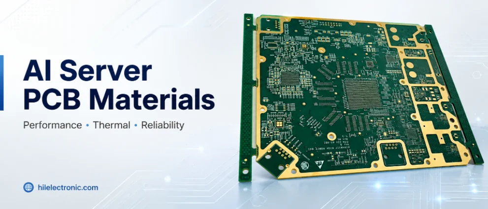
AI server boards carry very high power density. GPUs, accelerators, high-speed switches, memory devices, VRMs and optical or networking modules can create localized hot spots. PCB material selection affects how the board handles heat mechanically and electrically, even when the main cooling method is a heat sink, cold plate or liquid cooling system.
Power delivery and copper planning
High-current power delivery requires low-resistance copper planes, careful via design and sufficient decoupling. For AI accelerator and GPU boards, copper planning is not only about ampacity. It also affects board thickness, lamination balance, drilling, plating, etching uniformity, warpage and soldering performance.
Key power-delivery material considerations include:
- Inner-layer copper weight and plane distribution.
- Voltage drop and DC resistance of power paths.
- Thermal rise around VRMs, GPU power pins and high-current connectors.
- Via count, via size, plating thickness and current-sharing behavior.
- Whether heavy copper layers cause resin starvation or lamination voids.
Z-axis CTE and plated-through-hole reliability
High layer count AI server PCBs can be vulnerable to via fatigue because the plated copper barrel and the laminate expand at different rates during thermal cycling. Materials with lower and more controlled Z-axis CTE help reduce stress on plated through holes and vias. This is especially important for thick backplanes, midplanes, switch boards and accelerator boards that see repeated heating and cooling during operation.
Thermal vias, copper coins and local heat paths
Some AI server boards require thermal via arrays, heavy copper areas, copper coins, metal inserts or localized thermal spreading features. These structures must be planned with the material and lamination process. A copper coin or heavy copper area can help remove heat, but it can also create CTE mismatch, soldering imbalance or flatness issues if it is not designed for manufacturability.
Moisture absorption and reflow reliability
Low moisture absorption is important for high-reliability AI server PCBs. Moisture inside the laminate can increase the risk of delamination, measling, blistering or other thermal stress defects during soldering. This becomes more important when the board is thick, high layer count, hybrid material or assembled with large BGAs and high thermal mass components.
Manufacturing and PCB Assembly Considerations
A material that looks excellent in a datasheet can still fail in production if it is difficult to fabricate or assemble. AI server PCB materials must be evaluated together with the full manufacturing process: drilling, desmear, plating, imaging, etching, lamination, back-drilling, surface finish, solder mask, routing, electrical testing and final PCB assembly.
PCB manufacturing risks
| Manufacturing item | Why it matters for AI server PCB materials |
|---|---|
| Drilling and desmear | Low-loss resin systems, high glass content or specialty materials may require adjusted drilling parameters and desmear chemistry. |
| Plating reliability | Thick boards and high aspect ratio vias need strong plating control to avoid barrel cracks, voids or reliability failures. |
| Back-drilling | Via stubs can damage high-speed channel performance. Back-drill depth tolerance must match the stack-up design. |
| Impedance control | AI server boards need controlled dielectric thickness, copper thickness and etching compensation to meet impedance targets. |
| Lamination registration | High layer count and hybrid materials increase registration difficulty. The manufacturer must control scaling and press behavior. |
| Surface finish | ENIG, ENEPIG, immersion silver or other finishes should be selected based on BGA assembly, connector needs, shelf life and reliability. |
PCB assembly risks
Because Highleap Electronics provides both PCB manufacturing and PCB assembly, material review should also include the PCBA process. A thick AI server board with large BGAs, heavy copper, high thermal mass connectors and sensitive high-speed components may require a customized reflow profile and careful warpage control.
- BGA warpage: Large GPU, CPU, FPGA or switch packages need good board flatness and stable reflow control.
- Thermal mass imbalance: Heavy copper areas and large connectors can create uneven heating during soldering.
- Moisture control: Baking, storage and handling may be needed for high-reliability or moisture-sensitive builds.
- Cleanliness: High-density boards may require strict ionic contamination control to reduce leakage and CAF-related risks.
- Inspection: X-ray inspection is important for BGA, via-in-pad and hidden solder joints.
- Rework limitation: Reworking large BGAs on high-value AI server boards must be planned carefully because repeated heat exposure can stress the laminate.
Best practice: For AI server projects, do not separate PCB fabrication and PCB assembly decisions too late. The laminate, board thickness, surface finish, BGA package, reflow profile and inspection plan should be reviewed together before pilot production.
Supply Risk, Cost Control and Second-Source Planning
AI server PCB materials are often more difficult to source than standard laminates. High-performance CCL, specialty prepreg, HVLP copper foil and specific glass styles may have longer lead times, minimum order quantities or allocation limits. A design that depends on one rare material with no approved substitute can delay a complete hardware program.
The safest approach is to create a material strategy during the design phase, not after the Gerber files are finished. This strategy should include a preferred material, an approved alternative, availability review, cost comparison and electrical confirmation.
| Cost or supply issue | How to reduce risk |
|---|---|
| Ultra-low-loss material is expensive | Use it only on layers that require it. Consider a hybrid stack-up for lower-speed layers. |
| Specified material has long lead time | Approve a second source early and confirm electrical equivalence with stack-up calculation or SI simulation. |
| Copper foil option is unavailable | Check whether an equivalent VLP/HVLP foil is available and whether the loss model must be updated. |
| Material thickness does not match impedance | Ask the PCB manufacturer to propose available core/prepreg combinations before routing is locked. |
| Prototype uses one material but production needs another | Avoid changing material after validation unless the stack-up, impedance and SI performance are rechecked. |
Second-source qualification does not mean simply replacing one brand with another. It means confirming that the substitute material can meet the same electrical, thermal, mechanical and manufacturing requirements. For AI server PCBs, even small differences in dielectric thickness, Dk, Df, copper roughness or resin behavior can change the final result.
What to Send Highleap Electronics for a Material Review
To recommend the right AI server PCB materials, Highleap Electronics needs more than a board outline or Gerber file. The earlier the material review starts, the easier it is to reduce cost, improve yield and avoid redesign.
For a fast and useful review, please send the following information:
- Board function: GPU board, accelerator card, switch PCB, backplane, motherboard, NIC, storage controller or power board.
- Target data rate: PCIe generation, Ethernet speed, SerDes rate, 112G/224G requirement or other high-speed interface.
- Estimated layer count and board thickness: Include any required impedance layers and power planes.
- Preferred material: If your design already specifies Megtron, Tachyon, Astra, specialty low-loss laminate, AGC, Shengyi or another laminate, provide the exact part number if available.
- Controlled impedance table: Single-ended and differential impedance, tolerance, reference layers and trace geometry if already defined.
- Stack-up or preliminary stack-up: Core/prepreg thickness, copper weight and high-speed layer assignment.
- BGA details: Pitch, ball count, package size, via-in-pad requirement and escape routing constraints.
- Power requirements: High-current rails, copper weight, thermal areas, connector current and voltage drop concerns.
- Assembly information: BOM, placement file, large BGA packages, thermal pads, reflow sensitivity and inspection requirements.
- Production plan: Prototype quantity, pilot build, mass production forecast and target delivery date.
Request an AI Server PCB Material and Stack-Up Review
Highleap Electronics can review your AI server PCB design for material selection, stack-up feasibility, controlled impedance, high-layer-count fabrication, HDI structure, thermal reliability and PCB assembly risk. If your project includes GPU, accelerator, HPC, networking, switch, backplane or high-speed server hardware, send us your design files for an engineering review before production.
AI Server PCB Materials FAQs
What is the best PCB material for AI server boards?
There is no single best material for every AI server board. GPU boards, accelerator boards, switch boards, backplanes, NICs and power boards have different requirements. Critical high-speed layers usually need low-loss, very-low-loss or ultra-low-loss laminates with smooth copper. Power or low-speed control sections may use high-Tg or modified FR-4 materials when the electrical and thermal requirements allow it.
Can AI server PCBs use standard FR-4?
Standard FR-4 may be acceptable for low-speed control, simple power or non-critical sections, but it is usually not suitable for long high-speed SerDes paths in AI server systems. For 112G, 224G or similar high-speed channels, the design normally needs a lower-loss laminate, smoother copper and better Dk stability.
Why are Dk and Df important for AI server PCB materials?
Dk affects impedance and signal propagation delay. Df affects dielectric loss. In AI server PCBs, high-speed channels operate at frequencies where dielectric loss and conductor loss can reduce signal margin. A stable Dk and low Df help maintain controlled impedance and reduce insertion loss.
What copper foil should be used for high-speed AI server PCBs?
High-speed AI server PCBs often use VLP, HVLP or other low-profile copper foils to reduce conductor loss. The smoother the copper surface, the lower the high-frequency conductor loss tends to be. The exact foil should be selected together with the laminate, signal speed, trace length and manufacturing process.
What is glass weave skew and why does it matter?
Glass weave skew occurs when two traces in a differential pair experience different dielectric environments because of the woven glass structure in the laminate. At high data rates, this can create timing mismatch and reduce eye margin. Spread glass, low-Dk glass, suitable prepreg style and routing strategy can help reduce this risk.
Are hybrid stack-ups suitable for AI server PCBs?
Yes, hybrid stack-ups are common when the design needs to balance high-speed performance and cost. The key is to place low-loss materials only where they are required and use more cost-effective materials elsewhere. However, hybrid materials must have compatible lamination behavior, CTE and manufacturing process windows.
What material properties should be checked besides Dk and Df?
Important properties include Tg, Td, T288, Z-axis CTE, moisture absorption, CAF resistance, peel strength, resin content, copper foil roughness, prepreg availability and compatibility with multiple lamination cycles. These properties affect fabrication yield, assembly reliability and long-term operation.
How early should material selection be discussed with the PCB manufacturer?
Material selection should be discussed before final layout whenever possible. For AI server PCBs, the material affects trace width, spacing, impedance, layer thickness, via structure, back-drilling and cost. If the material is changed after layout, the stack-up and signal integrity may need to be recalculated.
What files are needed for an AI server PCB material quotation?
For quotation and engineering review, send Gerber or ODB++ files, stack-up, impedance requirements, material preference, drill files, board thickness, copper weight, surface finish, BOM, pick-and-place file and assembly requirements. If the design is not final, a preliminary stack-up and interface speed information are still useful.
Can Highleap Electronics help with both PCB fabrication and PCB assembly?
Yes. Highleap Electronics supports PCB manufacturing and PCB assembly. For AI server and high-performance computing projects, reviewing fabrication and assembly together helps reduce risks related to material selection, board warpage, BGA soldering, thermal mass, inspection and production yield.

Recommended Posts

Taconic RF 35 vs RO4350B PCB
Table of contentsRF-35 vs RO4350B Procurement and...

TMM4 Filter PCB Manufacturing
TMM4 filter PCB manufacturing is controlled by the...

TMM3 PCB Manufacturing for RF Modules
TMM3 PCB manufacturing is most useful where the RF module...

TMM6 PCB Fabrication
TMM6 fabrication is the process-control page for a mid-Dk...
How to get a quote for PCBs
Let’s run DFM/DFA analysis for you and get back to you with a report. You can upload your files securely through our website. We require the following information in order to give you a quote:
-
- Gerber, ODB++, or .pcb, spec.
- BOM list if you require assembly
- Quantity
- Turn time
For PCBA services, please provide your BOM (Bill of Materials) and any specific assembly instructions. We also offer DFM/DFA analysis to optimize your designs for manufacturability and assembly, ensuring a smooth production process.