
Back to blog
How Blind Via PCBs Impact Electronics Manufacturing

Vias are a critical component in the functionality of a printed circuit board (PCB). They are essentially holes that connect different layers of a PCB electrically and thermally. Vias allow for the connection of traces, polygons, and pads across multiple layers of a circuit board, thereby optimizing space utilization. Among the various types of vias, blind vias play a significant role. This article explores blind vias in PCBs, providing insights into their definition, features, fabrication process, types, and applications.
Understanding Vias in PCBs
Vias are an essential element in the design and functionality of PCBs. They are essentially small holes that are either plated or drilled to establish electrical connections between different layers of a PCB. These connections are crucial for linking pads, traces, and components across various layers, allowing for the transmission of signals and power throughout the board.
One of the key functions of vias is to enable changes to signal layers by connecting components to signal traces or planes. This helps in routing signals efficiently and effectively within the PCB. Vias are typically coated internally with copper to create electrical connections within the insulating layers of the board.
It’s important to differentiate vias from plated through-holes (PTH), which serve a different purpose. PTHs are primarily used for connecting through-hole components on the board, whereas vias are used for establishing connections between different layers of the PCB.
In summary, vias play a critical role in the functionality and design of PCBs, enabling the efficient transmission of signals and power across different layers of the board. Understanding the different types of vias and their applications is essential for designing and manufacturing high-quality PCBs.

What Are Blind Vias in PCBs?
Blind vias are specialized types of vias that start from one of the external surfaces of a PCB and extend only to specific internal layers, without passing through the entire board. Unlike through-hole vias that connect all layers of a PCB, blind vias offer targeted connectivity between selected layers. This capability makes blind vias particularly useful in scenarios where optimizing space on the PCB is crucial.
The primary function of blind vias in PCB design is to maximize the number of connections between the external and internal layers while minimizing the need for additional routing traces. By doing so, blind vias contribute to more efficient layouts and reduce the overall complexity of the board’s design. For instance, blind vias can connect the top surface layer to the next layer beneath it, providing additional routing options and improving space utilization.

Features of Blind Vias
Blind vias, a type of via used in printed circuit boards (PCBs), offer several distinct features that make them valuable in PCB design:
Reduced trace width and space: Blind vias enable designers to reduce the width of traces and the spacing between them. This allows for increased routing density on the PCB, which can be crucial in designs with limited space.
More holes than a traditional board: Blind vias allow for more vias per unit area compared to traditional vias that span the entire thickness of the PCB. This increased via density provides greater design flexibility and can help optimize signal integrity and power distribution.
Higher pad density and wiring: Because blind vias only extend to certain layers of the PCB, they enable higher pad density and wiring density on the board. This can lead to more compact and efficient designs, especially in high-density applications.
Cost-effective solution: Despite their added complexity, blind vias can be a cost-effective solution for optimizing PCB designs. By reducing the number of layers required in a design, blind vias can help lower manufacturing costs while still meeting performance requirements.
Blind vias offer several key advantages in PCB design, including increased routing density, greater design flexibility, and cost-effectiveness. These features make them a valuable tool for designers looking to optimize the performance and efficiency of their PCB designs.
Fabricating Blind Vias in PCBs
Fabricating blind vias in PCBs requires adherence to specific guidelines to ensure proper functionality and reliability. Here is a detailed overview of the process:
- Initial PCB Fabrication Steps: The process begins with the fabrication of the PCB core, which forms the base structure of the PCB. This core is typically made of a substrate material such as FR-4.
- Rules for Blind Vias: When fabricating blind vias, several rules must be followed:
- Blind vias must start from either the top or bottom layer of the PCB.
- They should not pass through an odd number of layers.
- Blind vias should not traverse the entire thickness of the PCB.
- Blind vias should not start or end at the core or center of the PCB substrate.
- Creating Blind Vias: Blind vias are drilled or created in the PCB to connect the internal layers with the surface layer. Careful consideration should be given to the size and depth of the vias to ensure proper metallization quality and functionality.
- Vias Diameter and Depth: The diameter and depth of the blind vias are critical. The depth of the blind via should not exceed 1, as deeper vias may lead to distortion or other issues. Larger vias indicate a larger dielectric gap between PCB layers.
- Drilling Process: The blind vias are added to the PCB through a drilling process. It is important to ensure that the drill depth is adequate to create a strong connection without compromising the integrity of the PCB.
- Use of Drill File: A separate drill file is used to define the blind via hole. The size of the hole indicates the distance between the inner and outer layers of the PCB.
- Stacking PCB Layers: Prepreg material is used to stack the PCB layers together, ensuring that the blind vias are properly integrated into the PCB structure.
By following these guidelines and procedures, manufacturers can fabricate blind vias in PCBs effectively, ensuring optimal performance and reliability.

Types of Blind Vias
Blind vias come in different types, each with its own fabrication method and characteristics:
- Controlled-Depth Blind Vias: These vias are created similarly to through-hole vias but with a slight difference. The drill used to create the holes is set to penetrate only partially through the circuit board. Modern technology ensures that the features won’t come in contact with the drill. After drilling, the hole is plated with copper. While controlled-depth blind vias offer advantages, such as precise depth control, they may not always be the best option due to the requirement for sufficiently large holes.
- Laser-Drilled Blind Vias:Laser-Drilled Blind Vias: These vias are typically created after laminating the PCB, but before the outer layer undergoes etching and lamination. Various types of lasers can be used for creating these holes, with consistent results. Laser-drilled blind vias offer high precision and are suitable for complex PCB designs.
- Photo-Defined Blind Vias: The creation of these vias involves laminating a photosensitive resin to a core. The photosensitive sheets feature a pattern indicating where the holes should be made. The board is then exposed to light, causing the remaining material on the PCB to harden. Subsequently, the board is placed in an etching solution to remove the material from the holes. After plating copper in the holes, the PCB’s outer layer is created. Photo-defined blind vias offer precise control and are suitable for high-density PCB designs.
- Sequential-Lamination Blind Vias: These vias are created using a thin laminate, similar to the process for a two-sided PCB. Elements are formed on the side that will become the board’s second layer, with a copper sheet on the other side forming the first layer. While the sequential-lamination method offers some advantages, such as increased layer count and complexity, it is rarely used due to its high cost.
Each type of blind via has its own advantages and disadvantages, and the choice of which to use depends on the specific requirements of the PCB design.
Important Considerations about PCB Vias
When selecting a via type for your PCB design, several critical considerations should be taken into account to ensure optimal signal integrity, manufacturability, and reliability:
Signal Integrity: Vias, despite their short length, can significantly impact signal integrity, particularly in high-frequency applications. For example, a through-hole via connecting the top two layers in a ten-layer PCB traverses eight layers of metal, potentially causing interference. It is crucial to identify and address such issues to maintain optimal signal performance. Utilizing advanced PCB design tools such as Cadence Allegro can help detect and mitigate signal integrity problems before manufacturing.
Aspect Ratio:The aspect ratio of a via in a PCB is a critical factor that impacts its manufacturability, reliability, and cost. It is defined as the ratio of the diameter of the via hole (D) to the thickness of the PCB (H), which is equal to the length of the via barrel. A higher aspect ratio indicates a longer and narrower via, which can pose challenges during the plating process and affect the overall quality of the via.
During the plating process, the via holes are plated with copper to provide electrical connections between the layers of the PCB. The plating process involves several steps, including drilling the holes, cleaning the holes, applying a conductive carbon layer, and electroplating the copper. Larger aspect ratio holes are more challenging to plate because the chemical solution containing copper ions must flow into the hole, and longer barrels make it harder for the solution to reach the center of the barrel.
For holes with a diameter of 10 mil or above, an aspect ratio of 1:10 is typically acceptable, with a maximum board thickness of 3 mm. For smaller holes, such as 8 mil or 6 mil, lower aspect ratios are required, along with thinner PCBs. For example, an 8 mil hole may have an aspect ratio of 1:8, with a maximum board thickness of 1.6 mm.
In summary, the aspect ratio of a via is an important consideration in PCB design, as it affects the plating process, reliability, and cost of the board. Designers must carefully select the aspect ratio based on the hole diameter and board thickness to ensure a successful PCB fabrication process.
Routing Density: Dense areas of a PCB, particularly those containing high pin-count ball grid arrays (BGAs), require careful routing to prevent channel blockage. The strategic use of blind vias can be crucial in allowing escape routing for BGAs, ensuring that every pin is properly connected. It is essential to design routing planes and channels to avoid obstruction under such components.
Annular Ring: The size of the annular ring, the area of copper pad surrounding the drilled hole, is another critical consideration. A mechanical drill may deviate during drilling, potentially causing drill breakout if the annular ring is insufficient. Ensuring a sufficiently large annular ring helps prevent drill breakout and ensures reliable connections.
Taking these factors into consideration when selecting and designing vias for your PCB will help optimize signal integrity, manufacturability, and reliability, ultimately contributing to the overall success of your PCB design.
Making the Best Use of Vias for Your Design
Vias play a crucial role in PCB design, providing paths for thermal and electrical energy to transmit within layers. While most vias are round or circular, component pads to which they connect may vary in shape. Using a PCB design package with comprehensive via management functionality, such as Cadence’s Allegro PCB Editor, is essential for proper via selection.
For pads carrying current, via geometry is crucial in determining signal electrical parameters. Understanding current carrying requirements for your traces is key to ensuring vias can transfer signals with high fidelity, minimal loss, and within ampacity limits. Effective trace width and spacing are also important, as vias complete circuits between surface components.
Adhering to IPC-2222 standards for minimum hole sizes is essential. After determining the minimum hole size, IPC-2221 Standard equations should be used to determine pad diameter. It’s also advisable to minimize the number of vias used to avoid implications for board mechanical and electrical properties.
Collaboration with your PCB manufacturer is crucial for efficient board manufacturing. Drill hole capabilities may vary between manufacturers, especially regarding aspect ratio limitations and minimum hole size. Properly selecting via type and size is essential for creating designs that optimize space and meet performance objectives. Understanding the relationship between surface routing and routing to and through planes is also vital for effective routing.
Applications of Blind Vias in PCBs
Blind vias find widespread application in various critical areas of PCB design and manufacturing, including:
- Reducing PCB Layers: One of the primary applications of blind vias is to reduce the number of PCB layers required. By allowing traces to be routed from the outer layers to inner layers, blind vias enable designers to achieve the necessary connectivity without adding extra layers, thereby reducing overall board thickness and cost.
- BGA Breakout: Blind vias are commonly used to route traces from ball grid array (BGA) components to inner layers of the PCB. BGAs have a high pin count and require a large number of connections, which can be efficiently managed using blind vias to access inner layers for routing.
- Aspect Ratio Reduction: Blind vias play a crucial role in reducing the aspect ratio of PCBs. Aspect ratio refers to the ratio of the thickness of the PCB to the diameter of the drilled hole. By using blind vias, designers can reduce the thickness of the PCB, resulting in lighter and more compact boards.
- High-Density Interconnect (HDI) Boards: HDI boards require high routing density and power delivery capabilities. Blind vias are essential in HDI boards to achieve the necessary connectivity between layers while maintaining a compact form factor. HDI boards are commonly used in applications where space is limited, such as smartphones, tablets, and other portable electronic devices.
Overall, blind vias are a versatile and essential component of modern PCB design, enabling designers to achieve higher routing densities, reduce board thickness, and improve overall performance and reliability.
Conclusion
Blind vias are instrumental in enhancing PCB designs by offering more routing possibilities and minimizing the need for excessive layers. They bring numerous benefits, such as improved routing density, cost reduction, and increased design flexibility. It is crucial for PCB designers and manufacturers to comprehend the fabrication process, various types, and applications of blind vias to maximize design optimization, achieve superior performance, and ensure cost-effectiveness.

Related Articles
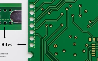
Mouse Bites PCB: A Complete DFM Guide for Panel Separation
Learn mouse bites PCB design rules, hole dimensions, spacing guidelines, and V-score comparison for reliable depanelization.
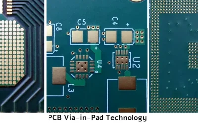
Comprehensive Analysis of PCB Via-in-Pad Technology
Explore the key advantages and challenges of Via-in-Pad technology in PCB design, with expert tips for maximizing performance and reliability.
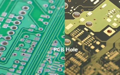
PCB Hole Selection to Optimize PCB Performance and Cost
Discover how to optimize your PCB designs with effective hole selection techniques like back drilling vs buried vias, mechanical vs laser drilling, and HDI stack planning to improve performance while minimizing manufacturing complexity and costs.