
Back to blog
Choosing the Best Via for Your PCB Layout

In the intricate landscape of PCB design, vias serve as crucial conduits for facilitating the seamless transmission of electrical signals across different layers of the board. As contemporary electronics continue to evolve with heightened complexity and component density, the utilization of diverse via types has become imperative. Among these, blind vias, buried vias, and micro vias emerge as pivotal components, each offering unique advantages and applications within the realm of PCB design. This comprehensive exploration delves into the nuances of these three via types, shedding light on their distinctive characteristics, applications, manufacturing considerations, and industry relevance.
Exploring Blind Vias in PCB Design
In the intricate realm of printed circuit board (PCB) design, blind vias emerge as a pivotal component, seamlessly bridging the gap between the outer layer of the PCB and one or more inner layers without penetrating the entire board. Aptly named for their concealed nature, blind vias offer a myriad of advantages, ranging from space-saving attributes to enhanced signal integrity, thereby revolutionizing the landscape of contemporary PCB layouts.
Advantages of Blind Vias
- Increased Density: By adeptly linking surface-mounted components to inner layers, blind vias unlock the potential for a more efficient utilization of board space. This optimization translates to tangible reductions in the overall size and weight of the PCB, a critical consideration in space-constrained applications.
- Reduced Layer Count: Blind vias serve as a catalyst for streamlining the PCB manufacturing process by mitigating the need for excessive layering. This reduction in layer count not only curtails manufacturing costs but also simplifies the intricate routing complexities inherent in multilayer PCB designs.
- Improved Signal Performance: Leveraging blind vias for signal routing yields a plethora of benefits, chief among them being the mitigation of signal degradation and electromagnetic interference (EMI). By curtailing the length of signal paths, blind vias foster optimal signal integrity and reliability, crucial imperatives in high-speed digital circuits.
Drawbacks of Blind Vias
- Manufacturing Difficulty: The realization of blind vias necessitates a meticulous orchestration of drilling and plating operations, thereby augmenting manufacturing costs and complexity. Precision is paramount in this regard, as inaccuracies in drilling or plating can compromise the vias’ functionality and reliability.
- Layer Count Restrictions: While blind vias offer a panacea for space-saving objectives, they inherently impose limitations on the maximum achievable layer count in a PCB design. This constraint necessitates a judicious balance between space optimization and the accommodation of requisite layers for routing and component placement.
Applications and Manufacturing Considerations
Blind vias find widespread application across a diverse array of PCB designs, ranging from high-density interconnect (HDI) boards to high-speed digital circuits. The imperative for space optimization is particularly pronounced in portable electronic gadgets such as smartphones and laptops, where every square millimeter of board real estate is meticulously optimized to accommodate a plethora of components within a confined space.
Manufacturing blind vias presents a confluence of challenges, chief among them being the imperative for precision drilling and plating operations. While traditional drilling techniques suffice for some PCB designs, the advent of laser drilling technology has revolutionized the landscape by endowing manufacturers with unparalleled precision and cost-saving benefits. However, designers must remain cognizant of the aspect ratio of the vias, as larger ratios may exacerbate manufacturing challenges and costs.
Blind vias epitomize a quintessential component in the modern PCB designer’s arsenal, facilitating the realization of compact, high-performance PCB layouts in the face of burgeoning complexity and component density. While their implementation entails inherent challenges, the manifold benefits they confer in terms of space optimization and signal integrity underscore their indispensable role in shaping the trajectory of contemporary electronics.

Buried Vias: Maximizing PCB Design Efficiency
Buried vias stand in stark contrast to blind vias, as they forge connections solely between two or more inner layers of a PCB, completely devoid of any association with the outer layers. This unique characteristic renders them invisible from either side of the board, thereby granting designers the freedom to allocate the outer layers for other critical purposes, such as component placement and trace routing, unimpeded by vias.
Advantages of Buried Vias:
- Increased Density: By seamlessly linking inner layers while bypassing the outer layers, buried vias unlock new levels of component density on the PCB, fostering more intricate and compact designs.
- Reduced Layer Count: The integration of buried vias can lead to a reduction in the number of routing layers required, translating to lower manufacturing costs and enhanced cost efficiency.
- Improved Signal Performance: Routing signals through buried vias mitigates signal interference, such as crosstalk and electromagnetic interference (EMI), thereby elevating signal quality and reliability.
While buried vias offer substantial benefits, they pose certain challenges, particularly in manufacturing. Precision drilling and plating operations are imperative for their successful implementation, albeit at the expense of heightened production costs and complexities. Accessibility issues may arise due to their concealed nature, making troubleshooting and repair challenging if they fail.
Applications of Buried Vias:
Buried vias find extensive application in high-density computing, telecommunications equipment, industrial control systems, and medical devices, where optimizing space and enhancing signal integrity are paramount. Their ability to streamline PCB layouts and enhance signal performance makes them indispensable in these demanding applications.
Buried Via Manufacturing Considerations:
The production of buried vias entails precise drilling and plating operations, which can escalate production costs. Designers must carefully consider the aspect ratio of the vias, as larger ratios may pose challenges and increase costs and manufacturing complexities. Furthermore, ensuring that the required number of buried vias has sufficient space on the board and does not interfere with other components or traces is crucial.
Buried vias represent a cornerstone of innovation in PCB design, offering a myriad of advantages in terms of space optimization, signal integrity, and design efficiency. Their strategic integration has revolutionized the landscape of modern electronics, enabling the creation of more compact, efficient, and high-performance electronic devices. By understanding the nuances of buried vias and their applications, designers can optimize their PCB designs and achieve superior performance in their electronic products.

Micro Vias: Revolutionizing PCB Design
The relentless drive towards miniaturization in the electronics industry has spurred the adoption of micro vias, heralding a new era of compact and efficient PCB designs. These tiny vias, with diameters of 150µm or less, have become instrumental in meeting the demands of modern electronics, enabling designers to achieve higher circuit densities and improved signal integrity in PCB layouts.
Advantages of Micro Vias:
- Increased Circuit Density: Micro vias allow for the creation of more connections in a smaller area, facilitating higher component densities on PCBs.
- Improved Signal Integrity: By shortening the length of interconnects, micro vias reduce signal loss and enhance signal integrity, critical for high-speed digital circuits and communication systems.
- Cost Efficiency: Micro vias can potentially reduce the number of layers required in a PCB, leading to lower production costs.
Manufacturing and Application of Micro Vias:
Micro vias are commonly used in high-density interconnect (HDI) PCBs, particularly in devices like smartphones, tablets, and portable electronic gadgets. Their small size allows for higher routing density and better signal integrity, making them ideal for fine-pitch surface-mount components such as ball grid array (BGA) and chip-scale package (CSP) devices.
Manufacturing micro vias typically involves laser drilling or other advanced techniques, which can be more expensive than traditional drilling methods. However, the benefits of improved performance and reduced board size often justify the additional cost.
Stacked Micro Vias:
Stacking micro vias further optimizes PCB designs by improving density and performance. Stacked micro vias provide a shorter, more direct path for electrical signals, reducing parasitic inductance and capacitance. This enhances signal integrity and can lower signal reflection and attenuation, improving overall performance in high-speed applications.
Considerations for Micro Via PCB Construction:
- Drilling: Drilling micro vias requires precise manipulation of laser settings to ensure the holes have the correct size and shape.
- Plating: Special plating procedures are necessary to ensure that micro vias are correctly connected to other PCB layers.
- Inspection: Non-destructive testing techniques may be needed to verify that micro vias are produced and connected appropriately.
- Material Selection: The reliability of micro vias is influenced by the materials used in their construction, necessitating the use of high-grade materials.
Micro vias have revolutionized PCB design, enabling the creation of smaller, more efficient, and higher-performance electronic devices. Their ability to enhance circuit density, signal integrity, and cost efficiency has made them indispensable in modern electronics, paving the way for further advancements in the field.

In the diagram, the via-to-copper clearance is 5.5 mils, and the minimum channel at the BGA is 5 mils. Without compromising channels, the only option is to reduce the size of small vias. This is one of the reasons why manufacturers often confirm via sizes, and it’s a factor that needs consideration during PCB design.
Understanding the Differences and Similarities Between Blind, Buried, and Micro Vias
In the realm of PCB design, vias serve as critical conduits for electrical signals between different layers of the board. Blind, buried, and micro vias are three types of vias that play distinct roles in PCB design, each offering unique advantages and challenges. Here, we delve into the similarities and differences between these types of vias to provide a comprehensive understanding.
Similarities:
- Space Saving: All three types of vias are designed to save space on the PCB compared to traditional through-hole vias. They enable a more efficient use of board real estate, allowing for increased component density and more complex PCB designs.
- High-Density Interconnects: Blind, buried, and micro vias enable higher-density interconnects, providing more routing options in high-density PCB designs.
- Size: Compared to traditional through-hole vias, all three types of vias are smaller in size, typically with diameters ranging from a few microns to a few tenths of a millimeter.
- Specialized Fabrication Techniques: Blind, buried, and micro vias require specialized fabrication techniques, such as laser drilling and plating, to create the desired via structures. This necessitates additional manufacturing steps and expertise, which can increase the cost and complexity of the PCB manufacturing process.
- Potential Impact on Signal Integrity: Depending on their placement and routing, all three types of vias can potentially impact signal integrity. Careful consideration of via placement and routing is necessary to minimize signal integrity issues.
Differences:
- Buried Vias: Buried vias connect two or more inner layers of a PCB without reaching the outer layer. They are entirely hidden within the board and cannot be seen from either side. This allows designers to use the outer layers of the board for other purposes without interference from vias.
- Blind Vias: In contrast, blind vias connect an outer layer of a PCB to one or more inner layers without penetrating the entire board. These vias are drilled from either the top or bottom of the board and are not visible from the opposite side of the PCB.
- Micro Vias: Micro vias are a more compact alternative to blind and buried vias. They are small vias with a diameter of 150µm or less and connect neighboring ring layers. Micro vias are drilled from the middle of the board using advanced techniques such as laser drilling.
- Production Complexity: The production of buried vias is typically more challenging, time-consuming, and expensive than the production of blind or micro vias. This is due to the additional manufacturing steps involved, such as sequential lamination and drilling.
Choose the best via for your PCB layout
When choosing the best via for your PCB layout, consider the specific requirements of your design, manufacturing capabilities, and budget constraints. Here’s a summary of the considerations for each type of via:
Tented Vias: These vias are covered with solder mask material to protect them from solder bridging and short circuits during the PCB manufacturing process. Tented vias are suitable for most standard PCB designs and offer good protection for the vias. They are cost-effective and straightforward to implement, making them a popular choice for many applications.
Blind Vias: These connect the outer layer of the PCB to one or more inner layers without penetrating the entire board. Blind vias are ideal for designs where space is limited and can help save on board real estate. However, they require precise drilling and plating operations, which can increase manufacturing costs.
Buried Vias: These connect two or more inner layers of the PCB without any connection to the outer layers. Buried vias are useful for increasing component density and reducing the number of routing layers needed. However, they are more challenging and costly to manufacture compared to blind vias.
Micro Vias: These are small vias with a diameter of 150µm or less, commonly used in high-density interconnect (HDI) PCBs. Micro vias allow for higher routing density and better signal integrity, making them suitable for compact and efficient PCB designs. However, they require advanced manufacturing techniques, which can increase production costs.
Consider the specific requirements of your PCB design, such as space constraints, signal integrity needs, and budget limitations, to determine the best via type for your project. Consulting with your PCB manufacturer can also help you make an informed decision based on your design specifications and manufacturing capabilities.
How to Find a Reliable Micro Via PCB Manufacturer?
To find a reliable micro via PCB manufacturer, start by researching online for companies with a strong reputation and experience in producing micro via PCBs. Shortlist manufacturers based on their capabilities, customer reviews, and compliance with industry standards. Evaluate their equipment, technology, and production processes to ensure they can meet your specific requirements.
Next, engage with the shortlisted manufacturers to discuss your project needs and assess their communication skills and responsiveness. Request samples or prototypes to evaluate their quality firsthand. Compare quotes from different manufacturers, considering factors such as quality, lead times, and additional services. Choose a manufacturer that offers competitive pricing without compromising on quality.
Finally, seek feedback from other customers or industry experts who have worked with the manufacturer. Consider visiting the manufacturer’s facilities to assess their capabilities, quality control measures, and overall professionalism. By following these steps and conducting thorough due diligence, you can confidently select a reliable micro via PCB manufacturer like Highleap Electronic that meets your project’s requirements and quality standards.
Conclusion
In the complex landscape of PCB design, vias play a crucial role in facilitating the seamless transmission of electrical signals across different layers of the board. With the evolution of electronics towards increased complexity and component density, the use of various via types has become essential. Blind vias, buried vias, and micro vias are key components, each offering unique advantages and applications in PCB design. Understanding the nuances of these three via types is crucial for optimizing PCB designs and achieving the best performance in electronic products.
Blind vias connect the outer layer of a PCB to one or more inner layers without penetrating the entire board, offering advantages such as space-saving attributes and enhanced signal integrity. Buried vias, on the other hand, connect two or more inner layers of a PCB without reaching the outer layer, enabling increased component density and reduced layer count. Micro vias, with diameters of 150µm or less, are ideal for designs with few layers and small components, offering benefits such as increased circuit density and improved signal integrity. Each via type has its own manufacturing considerations and applications, making it essential to choose the right type based on the specific requirements of the PCB design.

Related Articles
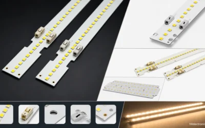
LED Linear & Strip Light PCBs: Long-Format Engines, Flexible & Rigid-Flex Boards
Build LED linear light PCBs for long rigid boards, flexible strips, rigid-flex lighting engines, RGBW control and even current distribution.

LED Grow Light PCBs: Multi-Channel Spectrum Boards, Drivers & Thermal Design
Manufacture LED grow light PCBs for full-spectrum engines, multi-channel drivers, thermal control boards and horticulture lighting assemblies.
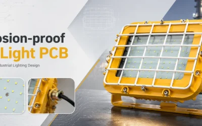
Explosion-Proof LED Light PCBs: Hazardous-Location Boards, Drivers & Assembly
Build explosion-proof LED light PCBs for hazardous-location fixtures, thermal MCPCB engines, potted drivers and surge control boards with Highleap.