
Back to blog
The Crucial Role of Filled Vias in Modern PCB Design

Comprehensive Classification of Filled Vias in PCB Design
In the realm of printed circuit board (PCB) design, the utilization of filled vias encompasses a diverse spectrum of options, each tailored to specific requirements and considerations. Let’s explore the various types of filled vias in detail:
1. Conventional Filled Vias: Conventional filled vias represent the foundational aspect of via technology, embodying a time-tested methodology for achieving robust interconnection within PCBs. This category involves the meticulous drilling of minute holes through the PCB substrate, subsequently filled with copper via an electroplating process. The deposited copper fortifies the inner walls of the via, with excess material meticulously removed to ensure a flat, uniform surface. Renowned for their reliability and versatility, conventional filled vias serve as a staple in the majority of PCB applications, offering scalability for large-scale production at economically viable costs.
2. Through-Hole Vias: Through-hole vias epitomize a fundamental means of establishing interlayer connectivity within PCBs, spanning the entire thickness of the board substrate. These vias are characterized by a bore that traverses all PCB layers, subsequently filled with copper to facilitate seamless current flow across diverse layers. Notably, through-hole vias excel in scenarios necessitating high-current transmission, owing to their robust construction that mitigates the risk of mechanical stress-induced disconnections. This inherent resilience makes through-hole vias a preferred choice for applications demanding steadfast electrical continuity and mechanical integrity.
3. Blind Vias: Blind vias represent a specialized category of filled vias that exhibit a truncated trajectory, terminating within the interior layers of the PCB substrate without penetrating its entirety. These vias are created by drilling from the PCB surface to predetermined interior layers, subsequently filled with copper to establish connectivity. Ideal for compact PCB layouts where space constraints preclude full via penetration, blind vias offer a cost-effective alternative to through-hole vias by minimizing drilling and plating requirements. Their inherent efficiency makes them a preferred choice for high-density PCB designs where spatial optimization is paramount.
4. Buried Vias: Buried vias constitute a discreet yet indispensable component of PCB design, facilitating interlayer connections within the confines of the PCB substrate without extending to its external surfaces. These vias are meticulously drilled through select interior layers of the PCB, subsequently filled with copper to ensure seamless interconnection. Particularly advantageous in multi-layer PCB configurations where extensive drilling through the entire board may compromise structural integrity, buried vias offer a pragmatic solution for preserving PCB functionality while minimizing manufacturing complexities and costs.
5. Microvias: Microvias epitomize precision-engineered vias characterized by their diminutive dimensions, boasting diameters of 0.15mm or less. Leveraging advanced laser drilling techniques, microvias are meticulously crafted to accommodate spatially constrained PCB layouts where conventional or blind vias may prove impractical. Following laser drilling, these micro-sized apertures are filled with copper via an electroless plating process, culminating in highly compact, yet resilient interconnections. Despite their enhanced performance capabilities, the intricate processing and specialized equipment required render microvias a premium solution, typically reserved for applications necessitating utmost miniaturization and performance optimization.
6. Stacked Microvias: Stacked microvias represent an advanced iteration of microvia technology, facilitating high-density interlayer connections within PCBs with limited spatial real estate. By stacking multiple microvias in close proximity, these vias enable unparalleled routing flexibility and signal integrity, making them indispensable for high-performance applications where space constraints mandate optimal resource utilization. The intricate drilling and filling process inherent to stacked microvias underscores their suitability for specialized applications demanding uncompromising performance within constrained form factors.
In essence, the comprehensive classification of filled vias underscores their pivotal role in enabling robust interconnection within PCBs, catering to a myriad of design considerations ranging from space optimization to signal integrity preservation. By judiciously selecting and integrating the appropriate type of filled vias, PCB designers can navigate the complexities of modern electronics design with confidence and precision.
If this requirement affects sourcing or production release, compare it with PCB design review and aluminum substrate PCB before sending the final files for review.

Advantages of Filled Vias in PCB Design
In the intricate world of printed circuit board (PCB) design, the strategic incorporation of filled vias yields a multitude of benefits, amplifying the reliability, performance, and manufacturability of electronic systems. Let’s delve into the comprehensive advantages offered by filled vias:
1. Enhanced Reliability
Filled vias serve as stalwart guardians of PCB integrity, bolstering reliability amidst dynamic environmental conditions. By fostering a robust interlayer connection, filled vias mitigate the adverse effects of temperature variations, mechanical vibrations, and moisture ingress. The filler material within vias alleviates stress concentrations, diminishing the likelihood of structural failure and ensuring uninterrupted functionality, even in the face of demanding operating conditions.
2. Superior Thermal Performance
The judicious integration of filled vias translates into augmented thermal dissipation capabilities within PCB assemblies. Through-filling materials exhibit superior thermal conductivity, facilitating efficient heat transfer across PCB layers. This phenomenon culminates in reduced operating temperatures, particularly advantageous in high-performance systems characterized by elevated thermal loads. Enhanced thermal management capabilities ensure prolonged component lifespan and sustained operational reliability, vital across diverse industries, including telecommunications, aerospace, and defense.
3. Enhanced Signal Integrity
Filled vias emerge as stalwart custodians of signal integrity, fortifying the fidelity of data transmission within PCB assemblies. By curbing signal losses and attenuating noise propagation, the filler material within vias ensures pristine signal propagation across diverse layers of the PCB. This heralds a realm of high-fidelity data communication, essential for applications mandating stringent performance criteria and immunity to electromagnetic interference (EMI).
4. Optimal Electrical Performance
Filled vias emerge as conduits of enhanced electrical performance, facilitating seamless current conduction across PCB layers. Whether imbued with conductive materials such as copper or non-conductive substances like epoxy, filled vias exhibit heightened electrical conductivity, attenuating voltage drops and enhancing power delivery efficiency. Copper-filled micro-vias, in particular, unleash a realm of enhanced thermal and electrical conductivity, coupled with reduced EMI susceptibility and heightened routing density, fostering the realization of compact yet potent PCB designs.
5. Amplified Design Density
The strategic integration of filled vias heralds a paradigm shift in PCB design density, enabling the accommodation of an expansive array of components within a confined footprint. Compared to conventional through-hole vias, filled vias occupy substantially less real estate on the PCB substrate, liberating valuable space for component placement and routing optimization. This heightened design density fosters the realization of intricate, feature-rich PCB layouts, vital for applications mandating maximal functionality within constrained form factors.
6. Cost-Effective Solutions
Despite initial investment considerations, filled vias emerge as prudent investments, heralding long-term cost savings and operational efficiencies. By streamlining PCB dimensions and curbing the incidence of failure, filled vias engender tangible reductions in material consumption and production costs. Moreover, their role in averting warranty claims and product recalls amplifies cost savings, fortifying the economic viability of PCB manufacturing endeavors.
7. Streamlined Assembly Processes
Filled vias expedite the PCB assembly process, imbuing it with a newfound level of efficiency and reliability. The filler material within vias furnishes robust support to mounted components, curtailing the risk of displacement or movement during assembly operations. Additionally, the structural reinforcement afforded by filled vias mitigates the likelihood of board damage, heralding expedited production cycles and tangible cost savings.
In summation, the judicious integration of filled vias heralds a realm of unparalleled benefits, transcending traditional paradigms to usher in a new era of reliability, performance, and manufacturability in PCB design. Leveraging the inherent advantages of filled vias empowers electronics designers to navigate the complexities of modern electronics with confidence and precision, unlocking a realm of innovation and functionality across diverse industry domains.

Via Filling Process in PCB Manufacturing
The via-filling process is a pivotal stage in printed circuit board (PCB) manufacturing, essential for ensuring robust interlayer connectivity and optimal board performance. This meticulous procedure involves filling via holes with either conductive or non-conductive material, facilitating seamless integration between the PCB’s various layers. Here’s an in-depth exploration of the key steps involved in the via-filling process:
CAM Engineering Verification: The process begins with CAM engineering verifying and inspecting the vias that require filling. Engineers treat these vias differently according to the production specifications. This step is crucial as it ensures the correct handling of vias, considering that the via-filling process differs significantly from conventional techniques. CAM engineering needs ample time to make changes to gerber files and ERP process flows, which can impact PCB progress. Confirming in advance enhances the first-pass yield and improves quality performance.
Preparing the Board: Before commencing the via-filling procedure, meticulous preparation of the PCB is imperative. The board undergoes thorough cleaning to eliminate any contaminants that could impede the adhesion and efficacy of the filling material. Even minute particles of dust or debris can compromise the integrity of the via connections, underscoring the importance of a pristine board surface.
Drilling the Holes: The next critical step entails drilling precise via holes into the PCB substrate. State-of-the-art computer-controlled drilling machinery ensures accuracy in bore diameter, depth, and placement, tailored to the specific requirements of the PCB design. The dimensions of the drilled holes are meticulously calibrated based on the board’s specifications and the intended mounting components, ensuring optimal interlayer connectivity.
Cleaning the Holes: Following the drilling process, thorough cleaning of the via holes is imperative to remove any residual debris or contaminants. Employing vacuum cleaners or high-pressure air pistols facilitates the expulsion of loose particles, ensuring unobstructed access for subsequent filling operations. This meticulous cleaning regimen is essential for maximizing the adhesion and integrity of the filling material within the via holes.
Applying the Filling Material: With the via holes primed and pristine, the application of the filling material commences. Depending on the specific requirements of the PCB design, the filling material may be either conductive or non-conductive in nature. Non-conductive fillers, such as epoxy resin, are commonly utilized to insulate and reinforce the via connections, while conductive fillers, comprising metals like copper or silver, facilitate seamless electrical conductivity between layers.
Curing the Material: Following the application of the filling material, the curing or hardening process is initiated to solidify the via connections. Various techniques, including heat application, UV light exposure, or chemical curing agents, may be employed based on the properties of the filling material utilized. This curing process ensures the establishment of a stable and reliable bond between the filling material and the walls of the via holes, fortifying the interlayer connections.
Finishing the Board: Upon completion of the curing process, the final stage involves the application of a protective coating or solder mask to the PCB surface. This additional layer serves to safeguard the board against environmental factors such as moisture, corrosion, and mechanical abrasion, enhancing its longevity and durability. Moreover, the smooth and uniform surface provided by the protective coating facilitates the seamless mounting of components, ensuring optimal functionality and performance of the assembled PCB.
In essence, the via-filling process represents a cornerstone of PCB manufacturing, epitomizing precision, reliability, and meticulous attention to detail. By adhering to stringent quality standards and leveraging advanced manufacturing techniques, PCB manufacturers can achieve unparalleled levels of interlayer connectivity and operational excellence in their products.
Advantages of Conductive Filled Vias
Conductive filled vias, particularly copper-filled micro-vias, offer several advantages in PCB design and manufacturing:
- High Routing Density: Micro-vias enable a high routing density on the PCB, allowing for a substantial reduction in overall PCB size and fewer layers. This results in cost savings due to material reduction and simplified manufacturing processes.
- EMI Reduction: By reducing the size and length of signal paths, micro-vias contribute to electromagnetic interference (EMI) reduction, resulting in improved signal integrity and reduced noise in electronic circuits.
- Better Thermal and Electrical Conductivity: Copper-filled micro-vias offer superior thermal and electrical conductivity compared to traditional vias. This enhances the efficiency of heat dissipation and ensures optimal electrical performance throughout the PCB.
Highleap Electronic utilizes micro-vias in their HDI (High-Density Interconnect) boards to achieve smaller form factors and lighter weights. The reduced form factor leads to shorter distances between components, reducing overall resistance and enhancing electrical conductivity. Additionally, the copper filling in micro-vias further reduces resistance, aiding in EMI reduction.
As surface-mount technologies (SMTs) continue to shrink in size, smaller pads are required for mounting them. Micro-vias, due to their diminutive size, are well-suited for increasing routing density, especially in via-in-pad designs aimed at close-pitch components like BGAs (Ball Grid Arrays).
Conductive filled vias excel in conducting heat away from hot components, facilitating efficient heat dissipation across the PCB. However, differences in the coefficient of thermal expansion (CTE) between the metallic fill and the surrounding laminate can lead to mechanical stress and potential fractures between the pad and the hole wall.
Despite these challenges, the benefits of conductive filled vias outweigh their drawbacks, making them a preferred choice for high-performance PCB designs requiring compact form factors, efficient heat management, and reliable electrical performance.
Filling Techniques in PCB Manufacturing
Various through-filling techniques are employed in printed circuit board (PCB) manufacturing, tailored to the specific needs of the board and the capabilities of the manufacturer. These techniques include:
- Plated Through-Hole (PTH) Filling: Plated through-hole (PTH) filling involves electroplating and depositing metal within via holes. This method begins by submerging the PCB in an electrolyte solution and applying an electrical current, typically using copper as the metal. Through electroplating, copper ions bond with the walls of the via holes, creating a strong and conductive link between the different layers of the board. PTH filling is widely used for its reliability and robust electrical connectivity, making it suitable for various PCB applications.
- Non-Conductive Epoxy Filling: Non-conductive epoxy filling utilizes epoxy resin to fill the via holes, forming a hardened connection with the hole walls. As epoxy glue is non-conductive, it does not impact the electrical characteristics of the board. This technique is often employed in non-critical applications where electrical conductivity is not a primary concern. Non-conductive epoxy filling provides insulation and reinforcement for the via connections, ensuring their integrity and reliability over time.
- Conductive Paste Filling: Conductive paste filling involves the use of a paste comprised of metal shavings suspended in a binder material. The paste is applied into the via holes, typically using screen printing techniques. Once applied, the paste dries and hardens, adhering to the walls of the via holes and forming a conductive pathway between the layers of the PCB. This technique is particularly useful for low-density boards where cost considerations are paramount. Conductive paste filling provides a cost-effective solution for achieving electrical connectivity while maintaining overall board performance.
Each filling technique offers unique advantages and is selected based on the specific requirements of the PCB design, desired electrical characteristics, and cost considerations. By leveraging these filling techniques, manufacturers can achieve optimal interlayer connectivity and ensure the reliability and performance of the finished PCB product.
Conclusion
PCBs are essential components in electronic devices, and vias play a critical role in their design. Vias are tiny holes drilled through copper layers on a PCB, plated with copper to create electrical connections between layers. Various types of vias, including through-hole vias, microvias, and via-in-pad designs, are used in PCBs.
Via filling, a PCB manufacturing process, involves filling these holes with a conductive or non-conductive material, such as epoxy, to improve signal integrity, heat management, and overall reliability. Copper-plated shut-filled vias represent a more advanced via filling technique, offering enhanced thermal conductivity and dissipation. PCB designers must carefully consider the type of vias and filling techniques best suited to their specific PCB design needs.
PCB & PCBA Quick Quote
Related Articles
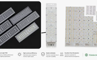
LED Tunnel Light PCB Manufacturing — High-Reliability Engines & Drivers
Build LED tunnel light PCBs for high-reliability luminaires, thermal MCPCB engines, dimmable drivers and corrosion-hardened outdoor assemblies.
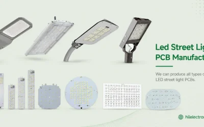
LED Street Light PCB Manufacturing & Assembly by Highleap Electronics
Get LED street light PCB fabrication and assembly for roadway luminaires, aluminum MCPCB engines, drivers and surge-protected control boards.
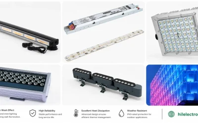
LED Wall Washer PCB Manufacturing — RGBW Light Engines & DMX Pixel Control
Manufacture LED wall washer PCBs for RGBW architectural fixtures, linear aluminum light engines, DMX controls and sealed outdoor assemblies.