
Gold Finger PCB Technology: A Complete Guide

What separates a correctly manufactured gold finger from one that will fail prematurely is not the gold itself — it is the plating specification, the nickel underplate thickness, the substrate chamfer geometry, the solder mask clearance, and the fabrication sequence that ensures the gold deposit reaches the correct thickness and hardness. This guide covers the engineering specifications and manufacturing process for PCB gold fingers, including the design rules that determine whether a gold finger connector will survive thousands of insertion cycles or fail within hundreds.
PCB Gold Finger — Key Specifications at a Glance
- Gold plating thickness: 1–3 µm electrolytic hard gold (standard); up to 0.76–1.27 µm for DDR5/JEDEC applications per MO-002
- Nickel underplate thickness: 3–6 µm (acts as barrier between gold and copper, prevents diffusion)
- Gold alloy: Gold-cobalt alloy (0.1–0.5% cobalt) for hard gold; significantly harder than pure ENIG soft gold
- Chamfer angle: 30°, 45°, or 60° bevel on the board edge — required for smooth connector insertion
- Solder mask clearance: Minimum 1mm clearance between gold finger pads and solder mask edge
- No vias in finger zone: Vias must be kept clear of the gold finger area to prevent plating bath contamination
- Insertion cycle rating: 1,000–10,000+ cycles depending on gold thickness and connector specification
Get a PCB Gold Finger Manufacturing Quote →
Table of Contents
- What Is a PCB Gold Finger and How Does It Work?
- Hard Gold vs. ENIG: Why Gold Fingers Cannot Use Soft Gold
- Gold Finger Plating Specifications: Thickness, Nickel, and Alloy
- Types of PCB Gold Fingers: Standard, Segmented, Stepped, and Long-Short
- PCB Gold Finger Design Rules: Chamfer, Clearance, and Layout
- How PCB Gold Fingers Are Manufactured: The Fabrication Sequence
- Applications: Where PCB Gold Fingers Are Used
- Quality Control and Testing for Gold Finger PCBs
- Frequently Asked Questions
What Is a PCB Gold Finger and How Does It Work?
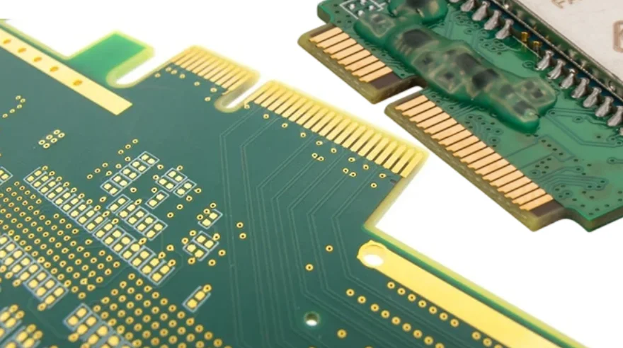
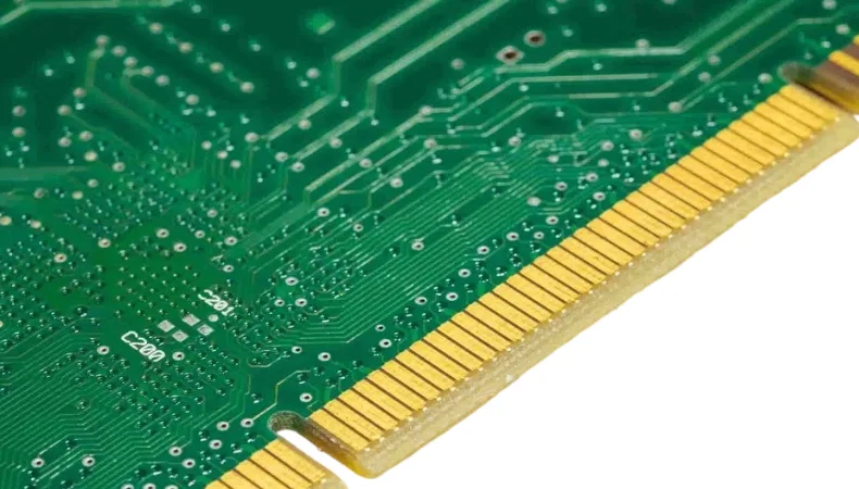
A PCB gold finger is a precisely spaced row of rectangular copper pads located at the edge of a printed circuit board, plated with electrolytic hard gold over a nickel barrier layer. The pads are arranged to match the contact pin pattern of a compatible edge connector or slot. When the board is inserted into the connector, the gold-plated pads make direct physical and electrical contact with the connector’s spring contacts, completing the circuit.
The gold plating serves two functions. First, gold’s electrical conductivity and its resistance to oxidation ensure that contact resistance remains low and stable — even after thousands of insertion and removal cycles and years of environmental exposure. Second, hard gold’s mechanical hardness (achieved by alloying with cobalt) resists the abrasive wear that occurs every time the board is inserted and withdrawn. Soft gold (pure ENIG) wears through to the nickel layer in as few as 10–20 insertion cycles under repeated use.
Gold fingers differ from the ENIG surface finish used on the rest of the board in a critical way: gold fingers use electrolytic (electroplated) hard gold, which can be deposited to precisely controlled thickness in the 1–3 µm range. ENIG uses immersion gold in the 0.05–0.15 µm range — far too thin for any mechanical contact application.
Hard Gold vs. ENIG: Why Gold Fingers Cannot Use Soft Gold
This is the most common question from engineers encountering gold finger PCB specifications for the first time: can ENIG be used for the gold finger contacts instead of hard gold? The short answer is no, and understanding why clarifies what the gold finger specification is actually controlling.
This difference creates a manufacturing requirement that separates capable PCB fabricators from those who cannot genuinely produce gold finger boards: the board must be processed with two different surface finishes in the same panel run. The component pads receive ENIG for solderability. The gold finger contacts receive electrolytic hard gold for wear resistance. This dual-finish process requires selective masking of the component pads during the hard gold plating step — a process control that not every PCB factory has implemented.
At Highleap Electronics, our dual-finish capability (ENIG body + electrolytic hard gold on the finger contacts) is a standard production process. We apply hard gold selectively to the gold finger area using precision masking, leaving the ENIG finish intact on the component pads. The result is a board that meets the solderability requirements of SMT assembly and the contact durability requirements of the edge connector simultaneously.
Gold Finger Plating Specifications: Thickness, Nickel, and Alloy
The plating specification for PCB gold fingers determines the performance envelope — contact resistance, wear life, and compatibility with the mating connector. The three parameters that matter most are gold thickness, nickel underplate thickness, and gold alloy composition.
Gold thickness
Standard gold finger applications specify 1–3 µm of hard gold. This range reflects the trade-off between cost (gold is priced by weight; thicker deposits cost more) and performance (thicker gold survives more insertion cycles before wearing through to the nickel). For applications with defined insertion cycle requirements, the appropriate thickness is determined by the connector manufacturer’s specification or the applicable IPC standard.
Specific application standards impose tighter ranges: DDR5 memory modules per JEDEC MO-002 specify 0.76–1.27 µm gold on a 3–5 µm nickel underplate. PCI Express edge connectors typically specify 30 microinches (0.76 µm) minimum gold thickness. Industrial backplane connectors with high cycle count requirements (10,000+ insertions) may specify up to 50 µm of electroplated gold (though this is rare and expensive; most applications fall in the 1–3 µm range).
Nickel underplate
The nickel layer between the copper pad and the gold deposit serves two functions: it acts as a diffusion barrier (preventing copper from migrating through the gold layer, which would degrade surface conductivity) and it provides a hard substrate that supports the thin gold overlay mechanically. Standard nickel underplate thickness for gold fingers is 3–6 µm. The nickel must be deposited before the hard gold plating step; it is not part of the ENIG process on the rest of the board.
Gold alloy composition
Hard gold for PCB gold fingers uses a gold-cobalt alloy containing 0.1–0.5% cobalt by weight. The cobalt addition increases the Vickers hardness from approximately 70 HV (pure gold) to 130–200 HV. This hardness increase is the mechanism behind the wear resistance — harder gold maintains its surface geometry under the repeated sliding contact that occurs during board insertion and removal.
Some specifications use gold-nickel alloys instead of gold-cobalt, particularly in applications where cobalt is restricted by environmental regulations. Gold-nickel hard gold achieves similar hardness levels and is an acceptable alternative where specified.
The single most common gold finger failure mode is using ENIG (0.05–0.15 µm soft gold) in place of electrolytic hard gold (1–3 µm). The ENIG deposit wears through to the nickel layer within 10–20 insertion cycles. Contact resistance rises, signals degrade, and the connection fails — even though the board looks correct at incoming inspection.
— PCB edge connector failure analysis
Types of PCB Gold Fingers: Standard, Segmented, Stepped, and Long-Short
Gold finger connectors are not a single geometry. Different applications require different pad arrangements, and the fabrication requirements vary accordingly.
Standard (uniform) gold fingers
The most common type — all pads are the same length and width, arranged in a single straight row at the board edge. Used in standardized interfaces: DDR memory, PCIe cards, M.2 drives, PCI expansion cards, and most industrial backplane connectors that follow a defined contact spacing standard. Fabrication is straightforward because the masking geometry is uniform.
Segmented gold fingers
Pads of different lengths arranged in a single row, creating a segmented appearance where some contacts are shorter than others. This geometry serves a functional purpose: in connectors with phased insertion, the longer contacts make electrical connection before the shorter contacts during board insertion. This allows power pins to connect before signal pins (preventing hot-insertion transients from damaging signal circuits) or enables board identification before full connection is established. Common in industrial module connectors, ruggedized backplane designs, and specialized telecommunications equipment.
Stepped (long-short alternating) gold fingers
A variation where contacts alternate between two different lengths in a defined pattern. Used in connectors that support two different insertion depths — a partial insertion position for low-power standby mode and a full insertion position for normal operation, for example. The stepped geometry requires careful fabrication to maintain the dimensional accuracy of both contact lengths.
Chamfered and beveled variations
All gold finger types require a beveled edge on the board (the chamfer that guides the board into the connector). Variations exist in the chamfer angle (30°, 45°, 60°) and whether the chamfer is applied to one side of the board or both sides (double-bevel). The connector manufacturer’s mechanical drawing defines the required chamfer geometry; the PCB fabricator applies it during the routing and beveling step.
PCB Gold Finger Design Rules: Chamfer, Clearance, and Layout
Gold finger PCBs require specific design rules that differ from standard PCB layout practice. These rules exist because the manufacturing process for gold fingers — particularly the edge beveling, selective masking, and plating sequence — creates constraints that standard DFM tools do not automatically enforce.
Board edge chamfer
The chamfer (bevel) at the gold finger edge of the board is not optional — it is required for the board to insert correctly into a slotted connector without damaging the connector contacts or the gold finger pads. Standard chamfer specifications:
The chamfer angle (measured from the board face) is typically 30°, 45°, or 60° depending on the connector specification. 45° is the most common default for PCIe and DDR connectors. The chamfer depth typically removes 0.5–1.0mm from each face of the board. Single-sided chamfer (one face only) is used for most consumer electronics interfaces. Double-sided chamfer (both faces) is used for applications requiring the board to be insertable in either orientation.
The chamfer is produced by the PCB fabricator during the board routing/profiling step. The Gerber files must specify the chamfer geometry explicitly — it cannot be assumed from the gold finger pad positions alone.
Solder mask clearance
Solder mask must not extend over the gold finger pads. The required clearance between the solder mask edge and the nearest gold finger pad is a minimum of 0.5mm, with 1mm being the standard recommendation. This clearance exists for two reasons: the solder mask is applied before the gold plating step, and any mask encroachment onto the pads would prevent the electroplating bath from reaching the full pad area; and in service, the connector contacts must make direct contact with the plated pad surface without any insulating mask material creating a barrier.
Via restriction in the gold finger zone
No vias should be placed in the gold finger area or within 1mm of the gold finger pads. Vias in the gold finger area create openings through which the electroplating bath can access inner copper layers, causing uncontrolled plating on inner layer copper and potentially causing shorts. They also create mechanical weak points near the board edge, where the board experiences repeated insertion forces.
Pad geometry and spacing
Gold finger pad width, length, and pitch are typically defined by the connector or slot specification rather than by the PCB designer. Key design rules that apply regardless of the specific connector standard: maintain consistent pad length across all contacts in the same row (unless implementing a segmented or stepped design); keep pad edges parallel to the board edge to within ±0.1mm; and maintain the pitch (center-to-center spacing) to within the connector specification tolerance, which is typically ±0.1mm for standard interfaces.
Connector keep-out and component clearance
The area surrounding the gold finger contact zone — the region that will be inside the connector body during insertion — must be kept clear of components, solder paste, and conformal coating. The depth of this keep-out zone is determined by the connector’s insertion depth specification. Typically a 5–15mm keep-out from the board edge into the board interior is required, depending on the connector type.
How PCB Gold Fingers Are Manufactured: The Fabrication Sequence
Understanding the manufacturing sequence for gold finger PCBs helps designers write correct fabrication notes and helps procurement engineers evaluate whether a factory can genuinely deliver the specified board. The process is more involved than standard ENIG fabrication because it requires an additional selective plating step and a mechanical beveling operation.
Step 1: Standard multilayer fabrication through outer layer copper
The board is fabricated through all standard steps of our PCB manufacturing process — inner layer imaging, lamination, drilling, plating, outer layer imaging and etching — through the point where the outer copper layers are complete. The gold finger pad areas are defined in the outer copper layer as standard copper pads.
Step 2: ENIG processing of component pads
The board receives ENIG processing — electroless nickel followed by immersion gold — on the component pads. The gold finger pad areas are masked during this step to prevent ENIG from being applied to the contacts that will receive hard gold. This selective masking step is where many factories without true dual-finish capability encounter difficulty.
Step 3: Solder mask application
Solder mask is applied to the board with the specified clearance around the gold finger pads. The mask is not applied over the gold finger contact areas. The mask is cured before the hard gold plating step.
Step 4: Electrolytic nickel and hard gold plating
The gold finger contact areas receive electroplated nickel (3–6 µm) followed by electroplated hard gold (1–3 µm or as specified). This is an electrolytic process requiring electrical current — the copper pads in the gold finger area are electrically connected to allow current flow during plating. Plating buses (thin copper traces connecting the gold finger pads to the board edge for electrical contact during plating) are typically required; these are routed to the board’s waste edge and removed during depanelization.
Step 5: Board profiling and edge beveling
The board is routed to its final outline, and the gold finger edge receives the specified chamfer using a beveling tool. The beveling operation is performed after plating to avoid contaminating the plating bath with routing debris. Chamfer angle and depth are verified against the specification. Board thickness at the chamfered edge is measured to confirm it matches the connector insertion tolerance.
Step 6: Electrical test and inspection
The finished board undergoes electrical continuity and isolation testing (flying probe or bed-of-nails). Gold finger contact resistance is verified using a four-wire Kelvin measurement if specified. Visual inspection of the gold finger area checks for plating uniformity, mask encroachment, and chamfer geometry. Gold thickness is typically verified by X-ray fluorescence (XRF) measurement on sample boards from each production lot.
Applications: Where PCB Gold Fingers Are Used
PCB gold fingers appear wherever a printed circuit board must make repeated, reliable electrical contact with a slotted connector. The specific applications span from consumer electronics to demanding industrial and defense environments.
Computer memory modules (DDR, SO-DIMM, DIMM)
DDR4 and DDR5 memory DIMMs are the highest-volume gold finger application. A DDR5 DIMM has 288 contacts on its edge connector, each plated to JEDEC MO-002 specification: 0.76–1.27 µm hard gold on 3–5 µm nickel. The high insertion cycle count in servers (modules are swapped during maintenance and upgrades) and the strict impedance requirements of DDR5 make correct plating specification critical.
PCIe, PCI, and expansion cards
GPU cards, NVMe drives, network adapters, and other PCIe expansion cards use gold finger connectors ranging from PCIe x1 (18 contacts) to PCIe x16 (164 contacts). The gold finger specification for PCIe typically calls for 30 microinches (0.76 µm) minimum hard gold. The PCIe connector specification requires beveling on both faces of the board edge.
M.2 and SATA drives
M.2 storage devices use a 67-pin edge connector with hard gold contacts. The M.2 form factor requires precise gold finger pad geometry to mate correctly with the M.2 slot’s spring contacts. M.2 modules are designed for infrequent insertion (typically one-time installation), so the insertion cycle requirement is lower — but the electrical contact reliability requirement is high because the interface runs at PCIe Gen 4/5 speeds.
Industrial backplane modules
Industrial PLC modules, VME cards, CompactPCI, VPX, and custom industrial backplane systems all use gold finger connections between modules and the backplane. Industrial applications often impose higher insertion cycle requirements (10,000+ cycles for frequently serviced modules) and wider operating temperature ranges than consumer applications, driving the need for thicker gold deposits (2–3 µm) and more robust nickel underplates. These boards are often supplied as fully assembled PCBA units ready for integration into rack systems.
Telecommunications and networking equipment
Line cards, optical transceivers, and blade server cards in telecommunications infrastructure use gold finger connectors. The combination of high data rates and high insertion reliability makes hard gold on these contacts a non-negotiable specification.
Medical and aerospace applications
Medical diagnostic equipment and aerospace electronics use gold finger connections where connector reliability directly affects safety. These applications often specify the thicker end of the gold thickness range and require documented traceability of the plating process, including XRF measurement records for every production lot.
Quality Control and Testing for Gold Finger PCBs
Gold finger boards require specific quality control steps beyond standard PCB inspection. The three most important are gold thickness measurement, contact resistance testing, and visual and dimensional inspection of the chamfer.
X-ray fluorescence (XRF) gold thickness measurement
XRF is the standard non-destructive method for measuring gold plating thickness on PCBs. An XRF gun directs an X-ray beam at the gold finger pad surface; the fluorescence spectrum of the returned signal identifies the elements present and their thickness. XRF measurement can resolve gold and nickel thicknesses simultaneously. We perform XRF sampling on every production lot of gold finger boards, with results documented in the shipping package. For applications requiring tighter process control (DDR5, aerospace, medical), 100% XRF measurement is available. Gold finger boards with HDI construction — combining fine-pitch BGA pads on the component area with gold finger contacts at the board edge — require XRF verification to confirm that the selective masking correctly separated the two plating processes without cross-contamination.
Contact resistance verification
For boards where the gold finger contact resistance specification is critical (high-frequency interfaces, low-current analog signals), contact resistance is measured using a four-wire Kelvin probe arrangement. The Kelvin method eliminates lead resistance from the measurement, giving a true reading of the contact interface resistance. Typical gold finger contact resistance is below 10 mΩ for a properly plated contact.
Insertion and withdrawal force testing
For gold finger boards produced in volume for a specific connector, insertion and withdrawal force testing on sample boards verifies that the board thickness, chamfer geometry, and pad width are within the connector’s mechanical specification. Boards that are too thick will not insert fully; boards with incorrect chamfer angles may damage the connector spring contacts.
Adhesion and wear testing
For applications with defined insertion cycle requirements, accelerated wear testing on sample boards can verify that the gold thickness specified will meet the cycle count target. This testing is typically performed by the connector manufacturer during connector qualification, but it may be requested by the PCB customer for new designs or new suppliers.
Highleap Electronics — Gold Finger PCB Manufacturing Capabilities
We manufacture gold finger PCBs with dual-finish processing (ENIG body + electrolytic hard gold on contacts), XRF thickness verification, and chamfer beveling on all board types from 2-layer through 20-layer. Our gold finger capability covers:
- Gold thickness: 1–3 µm standard; up to 50 µm electroplated for high-cycle applications
- Nickel underplate: 3–6 µm electroless nickel
- Chamfer angles: 30°, 45°, 60° single or double bevel
- Standards: DDR5/JEDEC MO-002, PCIe, M.2, industrial backplane formats
- XRF measurement records included in delivery documentation
- Selective masking for dual ENIG + hard gold finish on same panel
Frequently Asked Questions
What is a PCB gold finger?
A PCB gold finger is a row of gold-plated rectangular contact pads at the edge of a printed circuit board. When inserted into a compatible slot or edge connector, these pads form the electrical interface between the board and the host system. The term comes from their appearance — a row of parallel gold contacts resembling fingers. They are used in RAM modules, PCIe cards, M.2 drives, industrial backplane modules, and any other board-to-board connection that uses an edge connector format.
What gold thickness is used for PCB gold fingers?
Standard PCB gold finger specification calls for 1–3 µm of electrolytic hard gold (gold-cobalt alloy) over 3–6 µm of electroless nickel. DDR5 memory modules per JEDEC MO-002 specify 0.76–1.27 µm gold on 3–5 µm nickel. PCIe specifications typically call for 30 microinches (0.76 µm) minimum. Applications with high insertion cycle requirements (10,000+ cycles) may specify 2–3 µm of gold for increased wear life.
What is the difference between PCB gold fingers and ENIG?
Gold fingers use electrolytic hard gold (1–3 µm, gold-cobalt alloy, 130–200 HV hardness) deposited by electroplating to a precisely controlled thickness. ENIG uses immersion gold (0.05–0.15 µm, pure gold, 60–80 HV hardness) deposited by chemical displacement. ENIG is designed for solderability, not wear resistance — it fails as a contact surface within 10–20 insertion cycles. Gold fingers use hard gold specifically because it can withstand thousands of insertion cycles without wearing through to the nickel layer.
Why do PCB gold fingers require a chamfer (bevel)?
The chamfer at the gold finger edge of the board guides the board into the connector slot without catching on the connector’s spring contacts or scratching the gold surface during insertion. Without a chamfer, the board’s sharp edge would scrape the connector contacts, potentially damaging them and generating debris that degrades contact reliability. Standard chamfer angles are 30°, 45°, or 60° depending on the connector specification. The chamfer is machined by the PCB fabricator after plating, during the board profiling step.
Can ENIG be used for PCB gold fingers instead of hard gold?
No. ENIG (immersion gold, 0.05–0.15 µm) is far too thin and too soft for edge connector contact use. It wears through to the nickel layer within 10–20 insertion cycles, causing contact resistance to rise and signal integrity to degrade. Gold finger contacts require electrolytic hard gold (1–3 µm) with a gold-cobalt alloy composition for adequate wear resistance. A board specified as ENIG finish that is also used as a gold finger contact will fail prematurely in service.
What design rules apply to PCB gold fingers?
Key gold finger design rules: (1) No vias within 1mm of gold finger pads — vias allow the plating bath to reach inner copper layers. (2) Solder mask must have at least 0.5–1mm clearance from gold finger pad edges — mask encroachment prevents proper plating. (3) The board edge chamfer angle must match the connector specification — 30°, 45°, or 60°. (4) Gold thickness and nickel underplate thickness must be explicitly specified in the fabrication notes — “gold fingers” alone is not a sufficient specification. (5) No components or solder paste in the connector insertion zone, typically 5–15mm from the board edge.
How do you verify gold thickness on PCB gold fingers?
Gold thickness is verified by X-ray fluorescence (XRF) measurement — a non-destructive technique that measures the thickness of the gold and nickel layers simultaneously. XRF measurements are taken on sample boards from each production lot. For critical applications (DDR5, aerospace, medical), 100% XRF measurement on every board may be specified. The XRF measurement records should be included in the board fabrication documentation package.
What is the difference between segmented and standard gold fingers?
Standard gold fingers have all pads at the same length, creating a uniform edge contact row used in standardized interfaces like DDR memory and PCIe cards. Segmented gold fingers have pads of different lengths in the same row, so some contacts engage before others during board insertion. This phased engagement is used in connectors where power pins must connect before signal pins (protecting signal circuits from hot-insertion transients) or where board identification must occur before full connection. Segmented gold fingers are common in industrial backplane connectors and specialized telecommunications equipment.

Related Articles
Gerber vs ODB++ vs IPC-2581: Choosing a PCB Manufacturing Data Package
Compare Gerber vs ODB++ vs IPC-2581 and choose the best PCB manufacturing data package for fabrication, assembly, and fewer handoff errors.
How to Generate Gerber Files for PCB Manufacturing
Learn how to generate Gerber files in Altium, KiCad, and EAGLE, which outputs belong in the package, and how to avoid fab delays.
PCB Trace Width Calculator: How to Size Traces for Current, Voltage Drop, and Impedance
Size PCB trace width for current, voltage drop, internal and external layers, controlled impedance, and fabrication tolerance.