
DDR5 Module PCB Manufacturing Guide

Table of Contents
- Why DDR5 Module PCBs Demand a Specialized Manufacturer
- Layer Stack and Controlled Impedance Specifications
- Gold Finger Edge Connector: JEDEC MO-002 Requirements
- SMT Assembly for DDR5 DRAM and PMIC Packages
- RDIMM and LRDIMM: Additional Complexity
- Inspection and Testing from Bare Board to Finished Module
- What to Ask Before Placing a DDR5 Module Order
DDR5 is the memory standard powering 2024–2025 server platforms, AI workstations, and high-performance consumer systems. For hardware engineers and procurement teams sourcing DDR5 memory module PCBs — whether for branded DIMM production, server OEM supply, or custom industrial memory — the manufacturing requirements are significantly stricter than DDR4. Signal speeds starting at 4800 MT/s and reaching 7200 MT/s in production, combined with on-module PMIC regulation and tighter impedance windows, mean that a general-purpose PCB shop will produce modules that fail signal integrity validation before they ever reach a JEDEC compliance lab.
1. Why DDR5 Module PCBs Demand a Specialized Manufacturer
1.1 Structural Changes from DDR4 to DDR5
DDR5 introduced several architectural changes that directly impact PCB design and fabrication:
- On-module PMIC: DDR5 moves VDD and VDDQ regulation onto the DIMM itself. The PMIC handles local regulation, requiring the PCB to carry higher transient currents — placing thermal and copper weight demands on the board that DDR4 never imposed.
- Point-to-point CA bus: DDR5 replaces DDR4’s shared fly-by Command/Address topology with individual point-to-point routing to each DRAM device, increasing routing density and requiring individual length matching per device.
- Tighter timing margins: At 6400 MT/s, the DDR5 data eye is approximately 156 ps — half the margin of DDR4-3200. Any PCB-introduced impedance mismatch, crosstalk, or length error directly consumes this budget.
Manufacturers who routinely build high-density multilayer PCBs with tight dielectric control are better positioned to hold the trace geometry DDR5 demands across a production panel — not just on a prototype coupon.
1.2 Key Signal Groups on a DDR5 Module
- DQ/DQS: Data bus integrity determines sustained read/write throughput and error rate under thermal stress
- CK_t/CK_c differential clock: A single clock pair drives all DRAM on the module; any discontinuity propagates jitter to every device
- CA bus: Point-to-point routing means CA signals to each DRAM must be individually length-matched
- PMIC power routing: Low-impedance VDD/VDDQ planes must deliver clean rail voltage during 10–50A load transients
2. Layer Stack and Controlled Impedance Specifications
2.1 Typical 8-Layer UDIMM Stack
L1 — Top signal      : DQ routing, BGA fan-out, PMIC pads
L2 — GND plane       : Reference for L1 signal layer
L3 — Signal          : CA bus, auxiliary signals
L4 — VDD/VDDQ plane  : Power distribution
L5 — GND plane       : Reference for L6 signal layer
L6 — Signal          : CK, RAS/CAS routing
L7 — GND plane       : Return path continuity
L8 — Bottom signal   : DQ routing, passive component pads
The symmetrical GND-signal-GND arrangement on outer layers is standard practice. A manufacturer who cannot hold inner dielectric thickness to ±10% across the production panel will deliver boards with variable impedance — which shows up as random memory errors under load, not predictable failure. For DDR5 production, controlled-impedance fabrication with TDR coupon verification on every panel is non-negotiable.
2.2 Target Impedance Values
| Signal Group | Topology | Target Impedance | Tolerance |
|---|---|---|---|
| DQ bus | Single-ended | 40Ω | ±10% |
| DQS strobe | Differential pair | 85–100Ω | ±10% |
| CK_t / CK_c | Differential pair | 85–100Ω | ±10% |
| CA bus | Single-ended, point-to-point | 50Ω | ±10% |
| VDD / VDDQ planes | Plane | Low resistance | <10 mΩ rail-to-ball |
2.3 Minimum Fabrication Parameters
- Minimum trace width: 75 µm (3 mil) for DQ routing near x8 DRAM BGAs
- Minimum drill diameter: 0.20 mm for signal vias; 0.15 mm laser via for HDI RDIMM/LRDIMM variants
- Layer-to-layer registration: ±0.075 mm or better for 8-layer boards
- Base material: High-Tg FR-4 (Tg ≥ 150°C); Shengyi S1000H or equivalent halogen-free for lead-free assembly

3. Gold Finger Edge Connector: JEDEC MO-002 Requirements
3.1 Why Hard Gold — Not ENIG — Is Required
Every DDR5 DIMM has a 288-contact edge connector compliant with JEDEC MO-002. The contacts must use hard gold (electrolytic nickel-gold): 3–5 µm nickel underplate, 0.76–1.27 µm gold. Soft ENIG (immersion gold, typically 0.05–0.15 µm) wears rapidly under repeated slot insertions and builds contact resistance within 10–20 cycles. A board shop without a dual-finish process (ENIG body + electrolytic hard gold on the fingers) cannot produce JEDEC-compliant DDR5 modules.
Additional dimensional requirements:
- Chamfer angle: 45° bevel at the bottom edge, controlled to ±2°
- Key slot position: Within ±0.10 mm of JEDEC MO-002 drawing — these are CNC-routed, not scored
- Solder mask clearance: No mask encroachment onto the gold contact area
3.2 Common Gold Finger Defects to Screen For
- Solder mask bridging onto contact fingers → contact resistance failure
- Insufficient gold thickness (< 0.5 µm) → fails insertion cycle life testing
- Missing or mispositioned key slot → physically incompatible with DDR5 slot
- Incorrect chamfer → mechanical stress at PCB edge during insertion
4. SMT Assembly for DDR5 DRAM and PMIC Packages
4.1 Bill of Materials for a Standard DDR5 UDIMM
- 8–16× DRAM devices: FBGA-78 (x8) or FBGA-96 (x4) packages at 0.75–0.80 mm pitch (Samsung K4RAH, SK Hynix H5C, Micron MT60B series)
- 1× PMIC: BGA or QFN package handling VDD/VDDQ regulation (e.g., Renesas RAA229004, MPS MP2925)
- 1× SPD Hub: Serial Presence Detect hub with I3C interface (SPD5118 or compatible)
- Passives: 0201 and 01005 decoupling capacitors, series resistors, termination networks
The passive component density on a DDR5 UDIMM — particularly the 01005 decouplers — requires an SMT assembly line equipped for sub-millimeter component placement, not a generic mid-range production setup.
4.2 Moisture Sensitivity and Reflow Requirements
DDR5 DRAM packages are rated MSL-3: 168-hour floor life at ≤30°C/60%RH after opening dry packaging. Baking at 125°C for 24 hours is required if floor life is exceeded. Assembly lines without documented MSL controls produce boards with latent popcorning failures that appear in field use, not in final test.
Reflow profile targets for SAC305:
- Peak temperature: 245–255°C
- Time above liquidus (TAL): 45–60 seconds
- Ramp rate: ≤ 2°C/s preheat, ≤ 3°C/s ramp to peak
- Cool-down: ≤ 4°C/s (controlled cooling prevents solder joint microstructure damage)
4.3 BGA Placement Accuracy
FBGA packages at 0.75–0.80 mm pitch require pick-and-place accuracy of ±25 µm (3σ). A machine capable of ±50 µm — adequate for 1.0 mm pitch work — is insufficient; placement shift at 0.75 mm pitch causes BGA ball opens that are invisible to AOI and detectable only by X-ray. The inspection sequence after reflow should be: SPI → AOI → X-ray for all BGA packages → electrical test.

5. RDIMM and LRDIMM: Additional Complexity
Buffered DDR5 modules include a Register Clock Driver (RCD, e.g., Montage MTC10F2064 or Renesas RCD04) and optionally a Data Buffer (DB) for LRDIMM. From a manufacturing standpoint:
- Higher layer count: 8–10 layers needed to cleanly route CA/CS channels from the RCD to each DRAM array
- Additional BGA packages: RCD and DB chips at 0.65–0.80 mm pitch require the same fine-pitch placement and X-ray coverage as DRAM packages
- CA bus fan-out: The RCD re-drives CA/CS signals to all DRAM devices on the module — the fan-out routing is the most congested area of an RDIMM layout and drives the need for the extra signal layers
For LRDIMM designs, turnkey manufacturing that combines PCB fabrication and assembly under one roof eliminates the quality handoff risk between a bare board supplier and a separate assembly house — particularly important when layer count and BGA density are both elevated.
6. Inspection and Testing from Bare Board to Finished Module
6.1 PCB Fabrication QC
- TDR impedance report: Measured values from coupons on each panel — DQ (40Ω), DQS/CK (85–100Ω differential), CA (50Ω)
- AOI: Inner and outer layer inspection for trace defects and pad quality
- E-test: Flying probe continuity and isolation on every panel
- Microsection: Cross-section sample showing copper thickness, dielectric thickness, and via quality per production lot
6.2 Assembly and Module-Level Testing
- X-ray inspection: BGA joint verification for all DRAM, PMIC, and RCD/DB packages
- SPD programming and readback: Confirms the SPD hub is assembled correctly and the EEPROM is programmable
- Memory controller test: Enumeration in a reference platform, read/write pattern test at rated speed, thermal stress pass/fail
The full test sequence — from bare board TDR report through functional module-level electrical testing — closes the loop on every potential failure mode before modules are labeled and shipped.
7. What to Ask Before Placing a DDR5 Module Order
Before committing production volumes, get clear answers to these questions from any prospective DDR5 module manufacturer:
- What is your controlled impedance tolerance, and do you provide TDR coupon data with each shipment? ±10% is the DDR5 target; ±15% is DDR3-era tolerance.
- Can you produce dual-finish PCBs — ENIG body with electrolytic hard gold on the edge connector contacts?
- What is your placement accuracy for 0.75–0.80 mm pitch DRAM packages?
- Do you have in-house X-ray inspection? Outsourced X-ray means no real-time feedback loop into the assembly process.
- What is your MSL control procedure for DDR5 DRAM packages?
- Can you handle the full scope — fabrication through tested modules — from a single facility?
Highleap Electronics covers the complete DDR5 module manufacturing scope: controlled-impedance multilayer fabrication with TDR verification, dual-finish hard gold edge connectors, fine-pitch DRAM BGA assembly, in-house X-ray inspection, and functional module testing. Submit your design files for a manufacturing quote and we’ll provide a detailed cost and lead time breakdown, including a DFM review of your layer stack and edge connector specification.
Sabrina has over 18 years of experience in the PCB industry, with a strong background in CAM engineering and PCB file review. She supports PCB projects from prototype to volume production, focusing on manufacturability and process reliability. Her work helps engineering teams reduce production risk and achieve stable, high-quality PCB manufacturing results.

Recommended Posts

Wireless Mechanical Keyboard PCB Manufacturing
Table of contentsWireless Keyboard PCB Procurement...

Split Keyboard PCB Manufacturing & Assembly
Table of contentsSplit Keyboard PCBA Procurement...
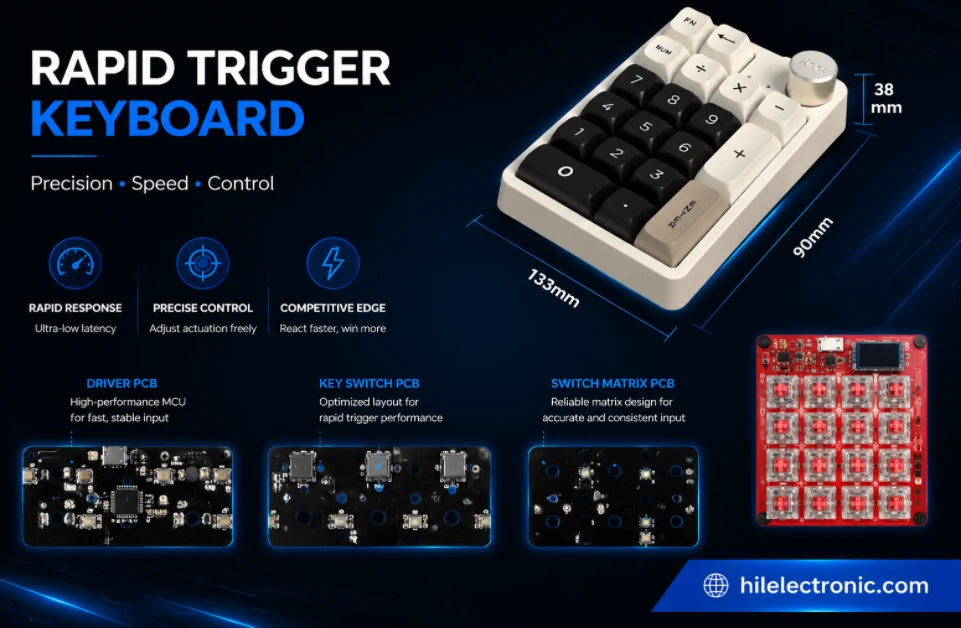
Rapid Trigger Keyboard PCB Manufacturing & PCBA
Table of contentsRapid Trigger PCBA Buying and Performance...
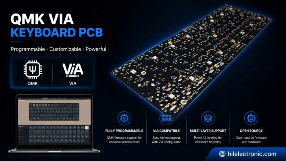
QMK/VIA Keyboard PCB Manufacturing & Assembly
Table of contentsQMK/VIA Keyboard PCB Buying...
How to get a quote for PCBs
Let us run DFM/DFA analysis for you and get back to you with a report.
You can upload your files securely through our website.
We require the following information in order to give you a quote:
-
- Gerber, ODB++, or .pcb, spec.
- BOM list if you require assembly
- Quantity
- Turn time
In addition to PCB manufacturing, we offer a comprehensive range of electronic services, including PCB design, PCBA (Printed Circuit Board Assembly), and turnkey solutions. Whether you need help with prototyping, design verification, component sourcing, or mass production, we provide end-to-end support to ensure your project’s success. For PCBA services, please provide your BOM (Bill of Materials) and any specific assembly instructions. We also offer DFM/DFA analysis to optimize your designs for manufacturability and assembly, ensuring a smooth production process.