
Blind and Buried Via PCB Quote Guide for HDI Boards

Our Blind and Buried Via PCB technology offers advanced manufacturing for high-layer, high-speed boards, ideal for industries like telecommunications, aerospace, and high-performance computing. Understand the key factors that influence cost and lead time in our detailed guide. Get a transparent, accurate quote tailored to your project’s unique requirements and accelerate your development process with precise, reliable results.
Table of Contents
- Understanding Blind and Buried Via Technology: Why Quote Complexity Increases
- What Information Do You Need to Provide for an Accurate Blind Buried Via PCB Quote?
- Quote Components: Breaking Down the Cost Structure
- HDI Stackup Configurations and Their Impact on Pricing
- Lead Time Considerations in Blind Buried Via PCB Quotations
- How to Evaluate and Compare Multiple Blind Buried Via PCB Quotes
- Getting Your Blind Buried Via PCB Quote from Highleap Electronics
A blind buried via PCB quote requires significantly more technical detail than a standard through-hole board quotation because the manufacturing process involves multiple sequential lamination cycles, precision laser or mechanical drilling at different stages, and complex layer registration requirements. Unlike conventional PCBs where a single quote parameter set suffices, blind and buried via boards demand stackup-specific information including which layers each via type connects, the drilling method for each via category, minimum finished hole sizes, aspect ratio limitations, and whether staggered or stacked via configurations are used. Understanding what drives the cost — and what information the manufacturer needs to provide an accurate quote — ensures you receive pricing that reflects actual manufacturing requirements rather than conservative estimates with large contingency margins.
Get Your Blind Buried Via PCB Quote Now
1. Understanding Blind and Buried Via Technology: Why Quote Complexity Increases
1.1 The Fundamental Difference That Affects Quotation
In a conventional PCB with only through-hole vias, the manufacturer drills the entire stackup after final lamination in a single drilling operation. The cost model is straightforward: board area × layer count × copper weight + drilling cost (holes × diameter factor) + plating + surface finish. Quote accuracy is high because the process variables are well-constrained.
Blind and buried via boards fundamentally change this model. A buried via connecting layers 3-6 in an 8-layer board must be drilled into the L3-L6 sub-composite before that sub-composite is laminated to the outer layer pairs. A blind via from L1 to L4 must be drilled after the outer layers are laminated but cannot penetrate beyond L4. This creates a sequential build process:
- Stage 1: Fabricate inner layer cores with buried vias
- Stage 2: Laminate cores with prepreg to build sub-assemblies
- Stage 3: Drill blind vias into sub-assemblies (laser or mechanical)
- Stage 4: Plate blind vias
- Stage 5: Laminate sub-assemblies to outer layers
- Stage 6: Drill through-holes (if any) through full stackup
- Stage 7: Impedance control verification and electrical testing
Each stage introduces process-specific costs, yields, and lead time. The manufacturer cannot provide an accurate quote without knowing the exact via interconnection scheme because each buried via layer pair requires a separate drilling and plating cycle, and each blind via configuration determines whether laser drilling (expensive, fast, small diameter) or mechanical drilling (lower cost, larger diameter, depth limitations) is feasible.
1.2 HDI Classification and Quote Implications
The IPC-2226 standard defines HDI complexity levels:
| HDI Type | Via Structure | Typical Quote Premium vs. Standard PCB | Primary Cost Drivers |
|---|---|---|---|
| Type I (1+N+1) | Single blind via from outer layer to first inner layer on one or both sides | 1.5–2.5× | One additional lamination cycle; laser drilling setup |
| Type II (2+N+2) | Two layers of blind vias on each side (L1-L2, L1-L3) | 2.0–3.5× | Two lamination cycles; sequential drilling; stacked via plating reliability |
| Type III | Buried vias in core + blind vias from outer layers | 2.5–4.5× | Buried via drilling/plating in cores; alignment precision; multiple lamination stages |
| Type IV | Multiple buried via layers + complex blind via structures | 3.5–6.0× | Multiple buried via stages; high aspect ratio challenges; yield risk |
| Type V/VI | Stacked and staggered microvias; any-layer interconnection | 4.0–8.0× | Advanced laser drilling; filled vias; multiple sequential builds; X-ray inspection |
When requesting a quote, you must specify the HDI type or provide a complete via interconnection table. A vague request for “8-layer HDI with blind vias” could describe a Type I board (moderate cost) or a Type VI board (4× higher cost). The manufacturer cannot quote accurately without this classification.
1.3 Why Generic “Per Square Inch” Pricing Doesn’t Work for Blind Buried Via Boards
Standard PCB quotes often use simplified formulas: base price per square inch × layer count multiplier × quantity discount factor. This approach fails for blind/buried via boards because:
- Via count dominates cost: A 50×50 mm board with 200 laser-drilled blind vias costs more than a 100×100 mm board with 50 blind vias, despite having 1/4 the area
- Lamination cycles scale non-linearly: Going from 2 lamination cycles (Type I) to 4 cycles (Type III) does not double the cost — it increases cost by 2.5–3× due to yield multiplication and process time
- Drilling method determines cost structure: Laser drilling has high setup cost but low per-hole marginal cost; mechanical drilling has low setup cost but higher per-hole cost due to tool wear and cycle time
A meaningful blind buried via PCB quote must be job-specific, calculated from actual stackup geometry and via interconnection requirements.
2. What Information Do You Need to Provide for an Accurate Blind Buried Via PCB Quote?
2.1 Essential Technical Data
Minimum required information for quote accuracy:
- Complete stackup: Layer count, copper weights per layer, dielectric thickness between layers, material type (standard FR4, high-Tg, halogen-free, or controlled Dk material)
- Via interconnection table: For each via type (through-hole, blind L1-L3, blind L8-L6, buried L3-L5, etc.), specify quantity, finished hole size, and pad size
- Drilling method preference: Laser, mechanical, or “manufacturer’s choice based on cost optimization”
- Via fill requirements: None, resin-plugged, copper-filled, or capped
- Aspect ratio limits: Maximum depth-to-diameter ratio you can accept (affects manufacturability and yield)
- Minimum trace/space: Especially critical on outer layers where blind via pads must fit between traces
- Surface finish: ENIG, immersion silver, OSP, or hard gold (affects blind via pad reliability)
- Quantity: Prototype (5–10), pilot (50–100), production (500+), and whether you anticipate repeat orders
- Quality class: IPC Class 2 or Class 3 (Class 3 requires 100% X-ray inspection of blind vias, adding significant cost)
2.2 Information That Significantly Affects Cost but Is Often Omitted
- Stacked vs. staggered vias: Stacked blind vias (where via on L1-L2 aligns directly above via on L3-L4) require via filling and planarization between lamination stages, adding $0.50–$2.00 per via. Staggered vias (offset by ≥0.3 mm) avoid this cost.
- Via-in-pad requirements: If vias must land inside BGA or QFN pads, they require copper filling and planarization — adding $0.20–$0.80 per via depending on diameter
- Back-drilling on through-holes: Often specified to remove via stubs on high-speed signals. Each back-drilled hole adds $0.005–$0.015 to the quote.
- Board thickness: If total board thickness is specified as a requirement (e.g., 1.0 mm ±0.1 mm), this constrains dielectric selection and may force thinner cores, affecting cost and manufacturability
- Impedance control: Controlled impedance on inner layers connected by buried vias requires modeling the via’s capacitive loading — some manufacturers charge for this engineering work
2.3 Optional Information That Enables Cost Optimization in the Quote
If you provide the following, the manufacturer can offer lower-cost alternatives:
- Design flexibility: “Can accept ±10% variation in finished board thickness” or “Via diameter can be 0.15–0.25 mm, designer’s preference was 0.20 mm but not critical” gives the manufacturer latitude to optimize material utilization
- Volume forecast: “Prototype now, 500/month in Q3” allows the manufacturer to suggest NRE amortization strategies or tooling investments that reduce per-unit cost at volume
- Lead time flexibility: “Prototype needed in 7 days, but production orders can be 15-day lead time” lets the manufacturer batch your production orders with other jobs, reducing setup cost
- Test requirements: If you have in-house electrical test capability, you may opt for visual inspection only at the PCB house, reducing the test line item

3. Quote Components: Breaking Down the Cost Structure
3.1 Line-Item Breakdown of a Typical Blind Buried Via PCB Quote
| Cost Component | Typical % of Total (Type I HDI) | Typical % of Total (Type III HDI) | What Drives This Cost |
|---|---|---|---|
| Base material | 20–30% | 15–25% | Copper-clad laminate, prepreg, material grade |
| Inner layer processing | 10–15% | 12–18% | Imaging, etching, AOI for each inner layer |
| Lamination cycles | 8–12% | 15–22% | Press time, alignment, multiple lamination stages |
| Drilling (laser + mechanical) | 15–25% | 20–30% | Laser drilling setup, pulse count, mechanical drilling, registration accuracy |
| Plating (copper, surface finish) | 10–15% | 8–12% | Electroless + electrolytic copper, ENIG/ImAg, plating thickness control |
| Outer layer processing | 8–12% | 6–10% | Outer layer imaging, etching, solder mask, legend |
| Testing and inspection | 5–8% | 8–12% | X-ray (blind via inspection), electrical test, impedance coupons, final inspection |
| NRE (engineering, tooling) | 10–18% | 8–15% | Stackup design, photo-tooling, drill programs, test fixtures (amortized over quantity) |
| Yield loss allocation | 5–10% | 8–15% | Scrap due to registration errors, blind via opens, delamination |
The key insight: in Type I HDI, drilling and lamination together represent 23–37% of cost. In Type III, they represent 35–52%. This is why via count and lamination complexity dominate the cost estimate.
3.2 Hidden Costs That Appear in Quotes But Aren’t Always Explained
- Registration tolerance adder: Blind/buried via boards require tighter layer-to-layer registration (±0.075 mm vs. ±0.15 mm for standard boards). Manufacturers achieve this with X-ray drill registration systems, which add a per-panel charge of $2–$8 depending on layer count.
- Micro-section analysis: For first-article or Class 3 boards, the manufacturer may perform destructive cross-sectioning of blind vias to verify barrel plating quality. This costs $50–$150 per sample and is sometimes included in NRE, sometimes as a separate line item.
- Impedance modeling: Buried vias create discontinuities in controlled impedance traces. Manufacturers with advanced DFM capabilities model the via’s capacitive loading and adjust trace width pre- and post-via to maintain impedance. This engineering work costs $100–$500 depending on complexity.
- Lamination press time premium: Multi-stage lamination ties up press capacity. During peak periods, manufacturers may charge a “capacity premium” of 5–15% for boards requiring more than two lamination cycles.
3.3 Volume Pricing and Quote Validity Period
Blind buried via PCB quotes are typically valid for 30–60 days due to material price volatility and press capacity allocation. Volume pricing breaks typically occur at:
- 5–10 pieces (prototype): NRE fully loaded, no material volume discount
- 25–50 pieces: NRE partially amortized, panel utilization improves
- 100–300 pieces: NRE negligible per unit, full panel utilization, material volume pricing kicks in
- 500+ pieces: Process optimization (batching multiple panels per lamination cycle), dedicated tooling, lowest per-unit cost
For recurring orders, manufacturers often offer “blanket PO” pricing where NRE is paid once and all subsequent orders within 12 months receive production pricing without re-quoting.
4. HDI Stackup Configurations and Their Impact on Pricing
4.1 Symmetric vs. Asymmetric Stackup Cost Difference
A symmetric stackup (same layer structure top and bottom) is easier to manufacture because:
- Lamination stress is balanced (reduces warpage risk)
- Drilling programs can use mirror symmetry (reduces setup time)
- Both sides can share the same blind via drilling setup
An asymmetric stackup (e.g., blind vias on top side only, no blind vias on bottom) saves the cost of bottom-side laser drilling but introduces warpage risk, requiring additional lamination press time and potentially thicker copper on the non-via side to balance stress. The cost difference is usually 5–10% higher for asymmetric stackups on 4-layer or 6-layer boards, negligible on 10+ layer boards where inherent stackup complexity dominates.
4.2 Sequential Build-Up Strategies and Quote Implications
Three common build strategies for complex HDI boards:
| Build Strategy | Process Flow | Cost Impact vs. Type I HDI | When Used |
|---|---|---|---|
| Core + blind vias (Type I/II) | Start with standard multilayer core, laminate buildup layers on both sides, laser drill blind vias | +50% to +150% | Most smartphone, tablet, and consumer electronics |
| Coreless build-up (ELIC) | Build entire stackup sequentially from center outward using only thin copper foil and resin | +200% to +400% | Ultra-thin boards (<0.4 mm), fine-pitch BGAs, package substrates |
| Mixed buried + blind (Type III) | Fabricate cores with buried vias, laminate cores together, add buildup layers with blind vias | +150% to +300% | High-layer-count HDI (10–20 layers), high-speed computing, telecom |
When requesting a quote, specify the build strategy if your design requires a specific approach. If you have flexibility, state “manufacturer’s choice for lowest cost” — some designs that appear to require Type III can be re-engineered as Type II with intelligent layer assignment, cutting cost by 30–50%.
4.3 Via Fill and Planarization: The Cost Multiplier for Stacked Microvias
Unfilled blind vias have an air cavity that limits reliability and prevents stacking. Via filling options:
- Resin plug: Fill via with epoxy resin. Cost: $0.05–$0.15 per via. Adequate for most applications. Enables one level of stacking (via on top of via).
- Copper fill (via plating): Electroplate copper to completely fill via. Cost: $0.20–$0.60 per via. Required for via-in-pad under BGA. Enables multi-level stacking. Requires planarization (additional $0.10–$0.20 per via).
- Conductive paste fill: Screen print conductive paste into via. Cost: $0.08–$0.25 per via. Used in low-cost consumer electronics. Less reliable than copper fill.
If your design has 500 blind vias and requires copper fill + planarization, that adds $150–$400 to the board cost. On low-volume orders this can dominate the cost estimate.
5. Lead Time Considerations in Blind Buried Via PCB Quotations
5.1 Standard Lead Time vs. Expedited Options
| HDI Type | Standard Lead Time | Expedited Lead Time | Expedite Fee |
|---|---|---|---|
| Type I (1+N+1) | 10–15 days | 5–7 days | +30% to +60% |
| Type II (2+N+2) | 15–20 days | 8–10 days | +40% to +80% |
| Type III | 18–25 days | 10–12 days | +50% to +100% |
| Type IV+ | 20–30 days | 12–15 days | +60% to +120% |
The lead time floor for blind/buried via boards is set by lamination cycle time (each lamination requires 1–2 days including press time and cool-down) and laser drilling capacity. Unlike standard PCBs where lead time can sometimes be cut by 50% with premium pricing, HDI lead times have a hard physical limit below which no amount of expedite fee can compress the schedule.
5.2 Lead Time Factors Outside the Manufacturer’s Control
- Material availability: Specialized high-Tg or low-Dk materials may have 2–4 week lead times from the laminate supplier. If your design requires Panasonic Megtron 7 or Isola Astra MT77, confirm material stock before assuming standard lead time.
- Laser drilling capacity: Laser drilling is a bottleneck in most HDI fabs. During peak season (Sept–Nov for consumer electronics), laser drilling queues can add 3–5 days to quoted lead time.
- X-ray inspection queue: Class 3 boards requiring 100% X-ray inspection of blind vias may face inspection queue delays during peak periods.
- Shipping: International shipping for prototypes can take 3–7 days. Expedited air freight adds $50–$200 depending on board dimensions and weight.
When requesting a quote, ask the manufacturer to specify which lead time components are firm and which are subject to material or equipment availability.
5.3 Design Decisions That Shorten Lead Time
- Use stocked materials: FR4 TG170 is stocked. Megtron 6 may require special order. Confirm material stock status.
- Avoid via fill: Unfilled blind vias eliminate one process step (2–3 days). If your design can tolerate unfilled vias, specify this.
- Accept Class 2 for prototypes: Class 2 inspection is visual + electrical test. Class 3 adds micro-section analysis and 100% X-ray, adding 2–4 days.
- Mechanical drilling for larger blind vias: If your blind via diameter is ≥0.20 mm and depth is ≤0.80 mm, mechanical drilling is faster than laser (no setup time) and may shave 1–2 days off lead time.

6. How to Evaluate and Compare Multiple Blind Buried Via PCB Quotes
6.1 Beyond Unit Price: Total Cost of Ownership
Three quotes for the same blind buried via board:
- Supplier A: $45/board, 12-day lead time, Class 2, visual inspection only
- Supplier B: $52/board, 15-day lead time, Class 3, 100% X-ray inspection, micro-section report included
- Supplier C: $38/board, 10-day lead time, Class 2, no X-ray inspection, “best effort” yield
The lowest unit price (Supplier C) may have the highest total cost if yield is poor. If 15% of boards fail electrical test at your assembly house, your effective cost is $38 ÷ 0.85 = $44.70/board plus the cost of re-ordering replacements and schedule delay.
Supplier B’s higher unit price includes verification that justifies the cost for production orders. Supplier A represents a middle ground suitable for prototypes where some yield loss is acceptable.
6.2 Quote Comparison Checklist
| Factor | What to Check | Why It Matters |
|---|---|---|
| Line-item transparency | Does quote break out material, drilling, lamination, NRE, testing separately? | Lets you identify which cost drivers you can influence through design changes |
| NRE handling | Is NRE a separate one-time charge or amortized into unit price? | Amortized NRE inflates prototype unit cost; separate NRE gives accurate production cost |
| Volume pricing | Does quote include pricing at 10, 50, 100, 500 pieces? | Shows whether supplier is prototype-focused or production-capable |
| Testing included | What testing is standard (electrical, impedance, X-ray)? What is optional/extra? | Testing costs can vary by 2–5× between suppliers |
| Tolerance specifications | What registration tolerance, impedance tolerance, thickness tolerance is quoted? | Tighter tolerances = higher cost. Confirm quote matches your actual requirements |
| Yield guarantee | Does supplier commit to delivering full quantity or “best effort”? | Some low-cost quotes assume 10–20% yield loss; you pay for 110 boards to get 100 good ones |
| Design support | Is DFM review included? Stackup optimization? Impedance modeling? | Engineering support can save 10–30% through design optimization |
| Lead time reality | Is quoted lead time firm or “estimated”? What is on-time delivery history? | Aggressive lead times may be marketing rather than realistic capability |
6.3 Red Flags in Blind Buried Via PCB Quotes
- Quote provided without requesting via interconnection table: Indicates the supplier is guessing at complexity rather than calculating from actual requirements
- No mention of X-ray inspection: Blind via quality cannot be verified visually. Absence of X-ray inspection in the quote suggests weak quality control
- Unit price that doesn’t decrease significantly from 10 to 100 pieces: Indicates NRE is being paid repeatedly rather than amortized
- Lead time shorter than industry standard for the HDI type: May indicate supplier is underestimating process complexity
- Quote valid for only 15–30 days: May indicate unstable material pricing or capacity constraints
Request Your Detailed Blind Buried Via PCB Quote
7. Getting Your Blind Buried Via PCB Quote from Highleap Electronics
Highleap Electronics specializes in complex HDI fabrication and provides transparent, itemized quotes designed for engineering decision-making:
7.1 Quote Request Process
- Upload Gerber + stackup documentation: Highleap’s automated DFM tool extracts layer count, via types, and interconnections
- Automated via classification: System categorizes through-hole, blind L1-Ln, buried Lx-Ly and flags any manufacturability concerns
- Drilling method optimization: For each via type, system recommends laser vs. mechanical based on diameter, depth, and cost
- Multi-quantity pricing: Quotes provided at 10, 25, 50, 100, 250, 500 pieces showing NRE amortization and volume discounts
- Alternative stackup suggestions: If your Type III design can be re-engineered as Type II with layer reassignment, Highleap engineering team provides cost comparison
7.2 What’s Included in a Highleap Blind Buried Via Quote
- Line-item breakdown: Material, inner layer processing, lamination cycles, laser drilling, mechanical drilling, plating, testing, NRE — each quoted separately
- Via-specific costs: Cost per blind via by diameter range, cost per buried via by layer span, via fill cost if applicable
- Testing scope: Standard (electrical + impedance coupon) vs. enhanced (add X-ray) vs. Class 3 (add micro-section), with pricing for each level
- Lead time transparency: Process timeline showing days allocated to inner layers, lamination cycles, drilling, plating, and testing
- Yield assumptions: Highleap quotes assume >98% yield and commits to full quantity delivery. If yield issues occur, replacements are provided at no additional cost.
- Design optimization recommendations: If panel utilization can be improved by 1–2 mm board dimension change, or if via placement allows staggered configuration instead of stacked (saving via fill cost), these are flagged with cost savings quantified
7.3 Expedited Quote Turnaround for Blind Buried Via Boards
- Standard quote turnaround: Within 24 hours for Type I/II HDI with standard materials
- Complex HDI quote: Within 48 hours for Type III/IV requiring engineering analysis
- Same-day quotes available: For urgent prototype requests with standard stackup configuration
7.4 Quote Validity and Pricing Lock
- Quote validity: 60 days for standard materials, 90 days if customer provides material stock consignment
- Blanket PO program: For recurring production, Highleap offers 12-month price locks on material and processing (NRE paid once, applies to all orders)
- Volume commitment discounts: If customer commits to 1,000+ boards over 12 months, additional 8–15% discount applied to production pricing
Highleap’s quote process is engineered to provide the technical transparency and cost optimization guidance that procurement teams need to make informed decisions on complex HDI boards.

Recommended Posts

Wireless Mechanical Keyboard PCB Manufacturing
Table of contentsWireless Keyboard PCB Procurement...

Split Keyboard PCB Manufacturing & Assembly
Table of contentsSplit Keyboard PCBA Procurement...
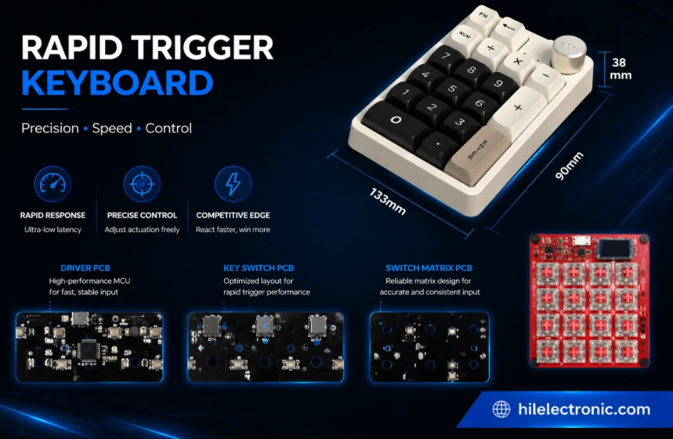
Rapid Trigger Keyboard PCB Manufacturing & PCBA
Table of contentsRapid Trigger PCBA Buying and Performance...
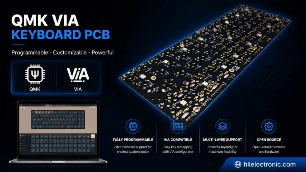
QMK/VIA Keyboard PCB Manufacturing & Assembly
Table of contentsQMK/VIA Keyboard PCB Buying...
How to get a quote for PCBs
Let us run DFM/DFA analysis for you and get back to you with a report.
You can upload your files securely through our website.
We require the following information in order to give you a quote:
-
- Gerber, ODB++, or .pcb, spec.
- BOM list if you require assembly
- Quantity
- Turn time
In addition to PCB manufacturing, we offer a comprehensive range of electronic services, including PCB design, PCBA (Printed Circuit Board Assembly), and turnkey solutions. Whether you need help with prototyping, design verification, component sourcing, or mass production, we provide end-to-end support to ensure your project’s success. For PCBA services, please provide your BOM (Bill of Materials) and any specific assembly instructions. We also offer DFM/DFA analysis to optimize your designs for manufacturability and assembly, ensuring a smooth production process.