
DBC Substrate Technology Design Materials and Power Module Applications

Table of Contents
- What Is a DBC Substrate?
- DBC vs Conventional PCBs: Where DBC Fits
- How DBC Substrates Are Manufactured
- Typical Applications in Power Electronics
- Key Advantages and Practical Limits
- DBC Ceramic Options: Al₂O₃ vs AlN vs Si₃N₄
- Copper Thickness, Patterning, and Design Constraints
- Surface Finishes and Assembly Compatibility
- DBC vs AMB vs DPC vs LTCC/HTCC
- How to Select the Right DBC Substrate
- Prototype to Volume: Reliability, Testing, and Quality Control
- RFQ Checklist: What to Provide for Fast, Accurate Quoting
- FAQ
What Is a DBC Substrate?
A DBC (Direct Bonded Copper) substrate is a ceramic power substrate where copper is directly bonded to one or both sides of a ceramic plate (commonly alumina, aluminum nitride, or silicon nitride). Unlike organic PCBs (e.g., FR-4) that rely on resin systems and laminated copper foils, DBC creates a robust copper–ceramic interface designed to minimize thermal resistance and withstand severe thermal cycling.
DBC substrates are typically used as the electrical and thermal base for power modules and high-power thermal platforms—supporting thick copper traces, high voltage isolation, and effective heat spreading from semiconductor devices to a heatsink or cold plate.
If you’re new to the technology, this overview of a direct bonded copper substrate explains the core structure and why it’s used for high-power thermal management.
DBC vs Conventional PCBs: Where DBC Fits
DBC substrates are often discussed alongside ceramic PCBs, but they are best understood as a power substrate rather than a general-purpose printed circuit board.
- Conventional PCBs (FR-4, high-Tg FR-4, PTFE, etc.) excel at dense routing, multilayer interconnects, and cost efficiency for signal/control electronics.
- DBC substrates excel at thermal management and high power density, especially where thick copper and ceramic isolation are needed.
In many products, DBC is integrated into a broader system: the control PCB manages logic and gate driving, while the DBC base supports the high-power switching devices (IGBTs/MOSFETs/SiC/GaN modules) and the power current paths. For conventional board builds and stackups, see our PCB fabrication services.
How DBC Substrates Are Manufactured
While process details vary by manufacturer, DBC production generally follows these stages:
- Ceramic preparation: ceramic plates are selected, cleaned, and prepared to ensure consistent surface condition and flatness.
- Copper bonding: copper sheets/foils are bonded to the ceramic using a high-temperature process under controlled atmosphere. The goal is a stable copper–ceramic interface with high bond strength and low thermal resistance.
- Patterning: the copper is patterned through photolithography and etching to form current paths, pads, and isolation clearances.
- Plating/surface finish: finishes are applied to match assembly needs (wire bonding, soldering, sintering, etc.).
- Final inspection and testing: dimensional checks, visual inspection, adhesion checks (as specified), electrical tests (as applicable), and documentation/traceability deliverables.
Because DBC involves ceramic handling and thick copper, manufacturability is influenced strongly by copper thickness, feature geometry, isolation requirements, and flatness/warpage control. A more detailed step-by-step breakdown is available in our DBC manufacturing process guide.

Typical Applications in Power Electronics
DBC substrates are widely used where thermal performance and isolation must be maintained over long life under high power cycling:
- IGBT and MOSFET power modules: motor drives, traction, industrial inverters, and power conversion.
- EV/HEV power electronics: traction inverters, on-board chargers (OBC), DC-DC converters.
- Renewable energy converters: solar inverters, wind power converters.
- High-power LED and laser platforms: chip-on-board (COB) LED arrays, high-brightness modules.
- Aerospace and defense: harsh thermal environments, vibration, long mission life requirements.
- Industrial power supplies and welding equipment: high current paths and robust thermal platforms.
Key Advantages and Practical Limits
| Capability | Why it matters | Practical considerations |
|---|---|---|
| Thermal performance | Lower thermal resistance helps reduce junction temperature and improve device reliability. | Material choice (Al₂O₃/AlN/Si₃N₄), copper thickness, and interface design influence performance. |
| High current paths | Thick copper supports high continuous and peak currents. | Thicker copper increases etch constraints and may impact cost, yield, and minimum feature sizes. |
| Electrical isolation | Ceramic provides strong dielectric isolation for high-voltage power stages. | Isolation clearance, creepage paths, edge design, and ceramic thickness must match voltage targets. |
| Thermal cycling reliability | Ceramic-based stacks can be more stable than organic laminates in thermal cycling. | Reliability depends on ceramic selection, copper thickness symmetry, layout stress concentration, and module assembly process. |
| Mechanical robustness | Important in vibration/traction applications. | Si₃N₄ is often selected when toughness and cycling performance are priorities. |
Limits to plan for: DBC is typically not used for high-layer-count routing, fine-pitch digital interconnects, or complex multilayer signal designs. It is a power/thermal platform—best paired with separate control PCBs when needed.
DBC Ceramic Options: Al₂O₃ vs AlN vs Si₃N₄
The ceramic base material is one of the most important performance and cost levers in DBC selection. For a deeper material-focused comparison, see DBC ceramic substrates.
Alumina (Al₂O₃)
- Strengths: cost-effective, widely available, mature manufacturing ecosystem.
- Typical use: many standard power modules where extreme thermal performance is not the limiting factor.
- Trade-off: lower thermal conductivity compared with AlN, so higher temperature rise may occur at very high power densities.
Aluminum Nitride (AlN)
- Strengths: high thermal conductivity; useful when thermal bottlenecks limit power density.
- Typical use: EV traction inverters, high power density modules, demanding thermal platforms.
- Trade-off: higher material cost and tighter process control requirements compared with Al₂O₃.
Silicon Nitride (Si₃N₄)
- Strengths: excellent mechanical toughness and strong thermal cycling performance; often preferred for high-reliability traction and vibration environments.
- Typical use: traction systems, railway, automotive modules where long cycling life is critical.
- Trade-off: typically higher cost than Al₂O₃; selection is driven by reliability and robustness needs.

Copper Thickness, Patterning, and Design Constraints
DBC commonly uses thicker copper than standard PCBs. This enables high current handling but introduces important patterning constraints:
- Minimum line/space: thicker copper generally requires wider traces and larger spacing due to etch factors.
- Edge definition: heavy copper etching can create undercut and sidewall profiles; pad geometries should consider manufacturing tolerances.
- Thermal stress: large copper areas can contribute to stress during thermal cycling; symmetry (top/bottom copper balance) may reduce warpage and stress concentration.
- Isolation design: voltage targets drive clearance and creepage requirements. Sharp corners and narrow gaps can increase risk of partial discharge in high-voltage environments.
Practical DFM checklist (layout stage)
- Define operating voltage and withstand voltage targets early (clearance/creepage rules follow).
- Specify copper thickness and confirm manufacturable line/space with the supplier before final routing.
- Avoid unnecessary large copper asymmetry between top and bottom layers.
- Use generous radii and avoid sharp internal corners in high-voltage clearances.
Surface Finishes and Assembly Compatibility
DBC substrates often serve as the base for power semiconductor attach and interconnect methods. Surface finish choice should match the downstream assembly process.
| Assembly need | Common finish considerations | Notes |
|---|---|---|
| Wire bonding | Finish compatible with aluminum/gold wire bonding requirements | Bondability is sensitive to surface condition, oxidation control, and cleanliness. |
| Solder attach | Finish that supports solder wetting and storage life | Thermal mass and copper thickness affect reflow profiling. |
| Sintering / advanced attach | Finish and surface planarity requirements may be stricter | Discuss attach method early to avoid rework and qualification delays. |
For high-reliability modules, cleanliness control, packaging method, and storage conditions can be as important as the finish itself.
DBC vs AMB vs DPC vs LTCC/HTCC
DBC is one of several ceramic-based technologies. Selection should be based on current, thermal requirements, feature resolution, and reliability targets.
| Technology | Best at | Typical applications | Main trade-offs |
|---|---|---|---|
| DBC | High current + strong thermal platform | Power modules, EV/industrial power | Less suited for very fine features |
| AMB (Active Metal Brazing) | Very strong bond, high reliability options | Ultra-reliability modules, thick copper needs | Higher cost; specialized process |
| DPC (Direct Plated Copper) | Finer pattern capability on ceramic | LED packages, smaller ceramic circuits | Often thinner copper; current capability may be lower |
| LTCC/HTCC | Multilayer ceramic circuits, embedded features | RF/microwave, complex ceramic modules | Not a direct replacement for heavy-copper power platforms |
How to Select the Right DBC Substrate
DBC selection is a multi-variable decision. A structured approach helps reduce redesign risk and speeds qualification. If you’re evaluating vendors, working with a specialized DBC substrate manufacturer can help align material choices, pattern constraints, and inspection requirements early in the project.
Step 1: Define thermal targets
- Power loss per device and allowable temperature rise
- Cooling method (heatsink, cold plate, forced convection)
- Interface strategy (TIM, baseplate configuration)
Step 2: Define electrical isolation requirements
- Operating voltage, surge/withstand requirements, safety margin
- Clearance/creepage needs based on environment and standards
Step 3: Define current profile
- Continuous current and peak current
- Thermal cycling and power cycling expectations
Step 4: Choose ceramic based on constraints
- Cost-sensitive: Al₂O₃ often fits
- Thermal-limited: AlN is commonly selected
- Reliability/toughness-limited: Si₃N₄ is often considered
Step 5: Align finish with assembly process
Confirm whether your downstream build uses wire bonding, solder, sinter, or other attach methods, then match finish and cleanliness requirements accordingly.
Prototype to Volume: Reliability, Testing, and Quality Control
Moving from prototype to volume production requires locking down the variables that most affect yield and reliability. If you need small-quantity builds for validation before ramp, a dedicated DBC substrate prototyping path helps confirm manufacturability and inspection expectations before production-scale commitments.
Reliability factors to control
- Bond integrity: stable copper–ceramic interface and consistent process control
- Flatness/warpage: impacts die attach quality and module assembly yield
- Thermal cycling design: copper geometry, symmetry, and stress concentration hotspots
- Surface condition: oxidation control and cleanliness for bonding/attach processes
Typical inspection and test options (as specified)
- Visual inspection: surface defects, edge quality, pattern integrity
- Dimensional inspection: outline, thickness, key features
- Electrical testing: continuity/isolation where applicable to patterned circuits
- Cross-section (if required): verification of structure and interface features for qualification lots
- Documentation: lot traceability and inspection records aligned to buyer requirements
RFQ Checklist: What to Provide for Fast, Accurate Quoting
DBC quotations vary widely because design and material choices drive both manufacturability and cost. Providing a complete RFQ package prevents back-and-forth and reduces quoting errors. If your project spans ceramic substrates and conventional boards, our ceramic PCB manufacturing overview can help you align process expectations across build types.
Required files
- Pattern files (Gerber or equivalent) for copper layers
- Mechanical outline (DXF preferred) and drawing notes
- Any special areas (keep-outs, mounting holes, critical clearances)
Required specifications
- Ceramic material (Al₂O₃ / AlN / Si₃N₄) and thickness
- Copper thickness (top/bottom; specify if different)
- Minimum line/space and minimum clearance targets (or voltage requirement to derive clearances)
- Surface finish requirement (and intended assembly method)
Commercial and planning inputs
- Prototype quantity and expected annual volume
- Target build stage (engineering prototype / pilot / mass production)
- Inspection/testing requirements and documentation needs
- Target delivery window and milestones
FAQ
1) What is a DBC substrate used for?
DBC substrates are used as thermal and electrical isolation platforms in power electronics. They commonly sit under power semiconductors in modules, transferring heat to a heatsink while maintaining electrical isolation and supporting high current paths.
2) Is DBC the same as a ceramic PCB?
DBC is a type of ceramic-based power substrate. It can be patterned like a circuit, but it is primarily used for power/thermal functionality rather than complex multilayer routing found in conventional PCBs.
3) How do I choose between Al₂O₃ and AlN for DBC?
Choose Al₂O₃ when cost and availability are primary and thermal requirements are moderate. Choose AlN when heat dissipation is the limiting factor and higher thermal conductivity is needed to reduce junction temperature.
4) When is Si₃N₄ preferred?
Si₃N₄ is often considered when mechanical toughness and long thermal cycling life are critical—such as traction and vibration-heavy environments—where durability and reliability drive the design.
5) What information most affects DBC lead time and cost?
Key drivers include ceramic type and thickness, copper thickness, feature geometry (line/space), surface finish, testing/documentation requirements, and quantity. Clear voltage/isolation targets also influence layout constraints and yield.
6) Can DBC support wire bonding and die attach?
Yes, but compatibility depends on finish selection, surface condition, and cleanliness control. It’s important to specify your attach and interconnect methods early so the finish and process controls match your assembly needs.
7) How does DBC compare to AMB?
DBC is widely used and cost-effective for many power applications. AMB may be selected for higher bond strength and certain high-reliability requirements, typically at higher cost and with different process characteristics.
8) What should I send in an RFQ to avoid delays?
Send copper pattern files, DXF outline, ceramic type/thickness, copper thickness, finish requirement, voltage/isolation targets (or minimum clearances), quantities for prototype and expected volume, and any testing/documentation requirements.

Recommended Posts

Wireless Mechanical Keyboard PCB Manufacturing
Table of contentsWireless Keyboard PCB Procurement...

Split Keyboard PCB Manufacturing & Assembly
Table of contentsSplit Keyboard PCBA Procurement...
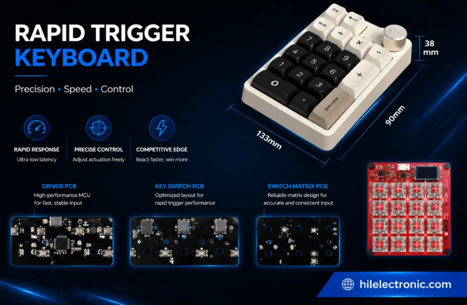
Rapid Trigger Keyboard PCB Manufacturing & PCBA
Table of contentsRapid Trigger PCBA Buying and Performance...
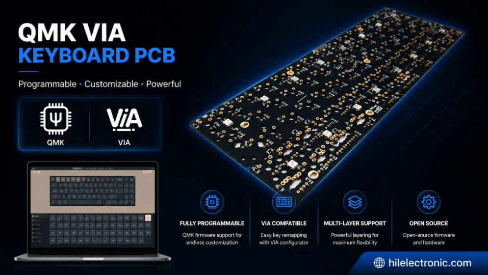
QMK/VIA Keyboard PCB Manufacturing & Assembly
Table of contentsQMK/VIA Keyboard PCB Buying...
How to get a quote for PCBs
Let us run DFM/DFA analysis for you and get back to you with a report.
You can upload your files securely through our website.
We require the following information in order to give you a quote:
-
- Gerber, ODB++, or .pcb, spec.
- BOM list if you require assembly
- Quantity
- Turn time