
Fast Turnaround Ceramic PCB Manufacturing

Table of Contents
- Why Most Turnaround Delays Originate on the Customer Side
- The Complete Design File Package for Instant Production Release
- Material Pre-Selection: Eliminating the Sourcing Bottleneck
- DFM-Ready Design Practices for Ceramic Substrates
- Communication Protocols That Prevent Schedule Slip
- Pre-Production Planning for Repeat Fast Turnaround
- Highleap’s Fast Turnaround Process
The biggest factor in achieving fast turnaround ceramic PCB delivery is not the manufacturer’s fabrication speed — it is the completeness and quality of your design submission. Analysis of delayed ceramic PCB orders consistently shows that 60–70% of schedule overruns originate in pre-production activities: incomplete files, ambiguous specifications, unanswered DFM questions, and slow PO approval. The fabrication process itself rarely exceeds its committed timeline once production starts.
This guide focuses on what engineers and procurement teams can control to achieve the fastest possible turnaround when ordering ceramic PCBs — front-loading the preparation work so production starts within hours of order receipt, not days.
1. Why Most Turnaround Delays Originate on the Customer Side
1.1 Root Cause Analysis of Delayed Orders
| Root Cause | Frequency | Typical Delay Added | Prevention |
|---|---|---|---|
| Missing or incomplete Gerber files | ~40% | 1–3 days | Use file checklist before submission |
| Ambiguous material specification | ~25% | 1–2 days | Specify exact material grade and thickness |
| Unclear metallization or finish requirements | ~15% | 1–2 days | Include complete fabrication drawing |
| Missing test or acceptance criteria | ~10% | 0.5–1 day | Define pass/fail criteria upfront |
| Customer unresponsive to DFM questions or quote | ~10% | 1–5 days | Designate authorized fast-response contact |
1.2 The Math of Pre-Production Delay
A rush order submitted on Monday morning with complete files enters fabrication by Monday afternoon. The same rush order with 3 DFM questions requiring customer confirmation enters fabrication Wednesday afternoon — if the customer responds within one business day per question. Three days of production capacity consumed by email exchanges, not furnace cycles.
2. The Complete Design File Package for Instant Production Release
2.1 Gerber and Manufacturing Files
- ☐ All copper layers (top and bottom for double-sided designs)
- ☐ Solder mask layers (if applicable for ceramic with solder mask — less common than FR4)
- ☐ Silkscreen / legend layer
- ☐ Board outline / mechanical layer with exact dimensions
- ☐ Drill file (Excellon format) with via positions and diameters
- ☐ Assembly drawing (if ordering assembled boards)
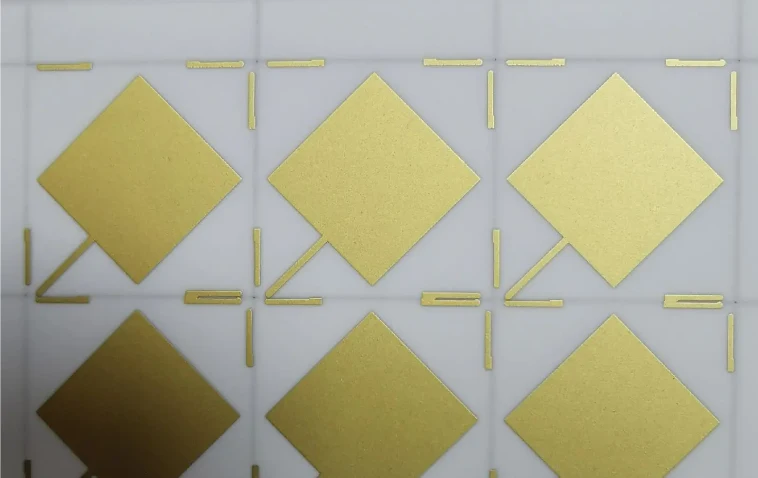
2.2 Fabrication Drawing Requirements
A proper fabrication drawing eliminates all ambiguity. It must specify:
- Ceramic material and purity grade (e.g., “Al₂O₃ 96%, Kyocera A-476” or equivalent)
- Substrate thickness (e.g., “0.635 mm ±0.05 mm”)
- Metallization method (DBC, thick film, thin film)
- Copper thickness (e.g., “0.30 mm DBC copper” or “15 µm thick-film Au conductor”)
- Surface finish type and thickness (ENIG, Ni/Ag, hard gold)
- Dimensional tolerances for critical features
- Electrical test requirements (continuity resistance, isolation voltage)
3. Material Pre-Selection: Eliminating the Sourcing Bottleneck
3.1 Stock Availability by Material
| Material | Typical Stock Status | Sourcing Lead Time (if not stocked) | Fast-Turnaround Strategy |
|---|---|---|---|
| Al₂O₃ 96% (0.25–1.0 mm) | Commonly stocked | N/A | No action needed — starts immediately |
| Al₂O₃ 99.6% | Sometimes stocked | 3–5 business days | Confirm stock before ordering; accept 96% if performance allows |
| AlN | Limited stock at most manufacturers | 5–10 business days | Pre-order substrates 2 weeks ahead; or prototype on alumina first |
| Si₃N₄ | Usually made to order | 2–4 weeks | Not compatible with fast turnaround unless pre-stocked by arrangement |
3.2 Advance Substrate Reservation
If you anticipate needing fast-turnaround ceramic boards on a recurring basis, arrange with your manufacturer to maintain a substrate buffer stock for your account. A small inventory investment (10–20 blank substrates) eliminates material lead time entirely for future urgent orders.

4. DFM-Ready Design Practices for Ceramic Substrates
4.1 Minimum Feature Rules by Metallization Method
Design within these limits to avoid DFM flags that require design revision and re-submission:
- DBC: Minimum trace width ≥0.15 mm; minimum space ≥0.15 mm; minimum via-to-edge ≥0.5 mm
- Thick film: Minimum trace width ≥0.30 mm; minimum space ≥0.25 mm; registration accuracy ±0.05 mm
- Thin film: Minimum trace width ≥0.025 mm; minimum space ≥0.025 mm (achievable with photolithography)
4.2 Common DFM Issues That Cause Revision Cycles
- Copper pattern too close to substrate edge — minimum 0.5 mm clearance required for singulation without copper damage
- Via-to-via spacing below process capability — increases risk of inter-via cracking during laser drilling
- Acute-angle trace junctions — create etching difficulties with thick DBC copper; use 45° or 90° junctions
- Text or silkscreen on ceramic — most ceramic processes do not support traditional silkscreen; use laser marking instead
A design that passes DFM review on first submission enters fabrication immediately. A design with 3 issues loses 1–3 days waiting for customer confirmation on each fix.
5. Communication Protocols That Prevent Schedule Slip
5.1 Single Point of Contact
Assign one person on your team who can answer DFM questions, approve quotes, and issue POs within hours — not days. Provide this person’s direct phone number and working hours to the manufacturer. The difference between “email response within 4 hours” and “email response within 48 hours” can shift your delivery by an entire week.
5.2 Pre-Approved Design Adjustments
Include a blanket approval with your order: “Minor DFM adjustments (trace width changes ≤0.02 mm, edge clearance additions ≤0.1 mm) are approved without separate customer confirmation.” This eliminates the approval round-trip for routine manufacturability adjustments that do not affect circuit function.
6. Pre-Production Planning for Repeat Fast Turnaround
If your product lifecycle requires periodic fast-turnaround ceramic orders (design iterations, small production batches, emergency replacements), establish these foundations:
- Qualified process baseline: First article inspection data and process parameters documented from the initial order, so repeat orders skip engineering setup
- Stored screen/stencil tooling: Thick-film screens and etching artwork retained at the manufacturer for immediate use on re-orders
- Blanket PO: Pre-approved pricing and terms so individual orders require only a release notice — no quote-approve-PO cycle
- Substrate reservation: Pre-purchased blank substrates stored at the manufacturer’s facility
With these elements in place, repeat orders can enter production within hours of the request.
Submit Files for Fast Turnaround
7. Highleap’s Fast Turnaround Process
Highleap Electronics optimizes every pre-production step to deliver the fastest achievable ceramic PCB turnaround:
- DFM response: 2–4 hours for complete file submissions; same-day for rush orders
- Quoting: Within 24 hours — same day for returning customers with established pricing
- Material stock: Al₂O₃ (96%, 99.6%) and selected AlN thicknesses maintained in inventory for immediate production
- Integrated assembly: On-site SMT assembly eliminates the transit gap between fabrication and assembly
- Shipping: Express courier access (DHL/FedEx/UPS) from our manufacturing facility with 2–3 day worldwide air freight
Sabrina has over 18 years of experience in the PCB industry, with a strong background in CAM engineering and PCB file review. She supports PCB projects from prototype to volume production, focusing on manufacturability and process reliability. Her work helps engineering teams reduce production risk and achieve stable, high-quality PCB manufacturing results.

Recommended Posts

TUC TU-872 SLK PCB for High-Speed FR-4 and CAF-Resistant Designs
TUC TU-872 SLK is a modified-epoxy FR-4 system designed to...

Shengyi S1000-2M PCB for High-Layer-Count Lead-Free Reliability
Shengyi S1000-2M is a high-Tg, low-CTE FR-4.0 laminate...
Isola P25N PCB for High-Temperature No-Flow Prepreg Bonding
A P25N project is not a routine request to replace one...
ITEQ IT-88GMW PCB for 76-81 GHz Automotive Radar Modules
A 76–81 GHz radar PCB cannot be designed as a scaled...
How to get a quote for PCBs
Let us run DFM/DFA analysis for you and get back to you with a report.
You can upload your files securely through our website.
We require the following information in order to give you a quote:
-
- Gerber, ODB++, or .pcb, spec.
- BOM list if you require assembly
- Quantity
- Turn time
In addition to PCB manufacturing, we offer a comprehensive range of electronic services, including PCB design, PCBA (Printed Circuit Board Assembly), and turnkey solutions. Whether you need help with prototyping, design verification, component sourcing, or mass production, we provide end-to-end support to ensure your project’s success. For PCBA services, please provide your BOM (Bill of Materials) and any specific assembly instructions. We also offer DFM/DFA analysis to optimize your designs for manufacturability and assembly, ensuring a smooth production process.