
DBC Substrates for Ceramic PCBs and Power Modules

DBC (Direct Bonded Copper) substrates are widely used in power modules and high-heat electronic designs where efficient thermal transfer and electrical isolation are critical. This page provides a practical overview of DBC structures, materials, manufacturing considerations, and how they compare with other ceramic PCB technologies.
Table of Contents
- 1) What Is a DBC Substrate?
- 2) How DBC Substrates Fit Into PCB Fabrication
- 3) Typical Applications of DBC Substrates
- 4) Key Performance Advantages
- 5) Ceramic Materials Used in DBC Substrates
- 6) DBC vs Other Ceramic PCB Technologies
- 7) Selecting the Right DBC Substrate Solution
- 8) Next Steps: Manufacturing, Prototyping & RFQ
At Highleap Electronics, we are a full-service PCB manufacturer providing ceramic PCBs, DBC substrates, metal core boards, multilayer PCBs, and complete PCB assembly services.
DBC substrates are one of the thermal management solutions we support for high-power and high-reliability applications such as power electronics, automotive modules, and industrial equipment. This guide explains how DBC technology works, when it should be used, and how it fits within broader PCB and ceramic PCB fabrication options.
Ready to explore our specialized capabilities? Visit our dedicated page for ceramic PCB fabrication or learn about our full PCB fabrication services.
1) What Is a DBC Substrate?
A DBC substrate, also known as a direct bonded copper substrate, is a type of ceramic circuit board in which copper foil is directly bonded to one or both sides of a ceramic base material through a high-temperature oxidation process. Unlike traditional PCB fabrication methods that rely on adhesive layers, DBC technology creates a metallurgical bond between the copper and ceramic, resulting in exceptional thermal conductivity and mechanical reliability.
The bonding mechanism involves heating copper and ceramic to temperatures near the copper-oxygen eutectic point (approximately 1065°C). At this temperature, a thin layer of copper oxide forms at the interface, which then reacts with the ceramic surface to create a permanent, high-strength bond. This process eliminates the need for intermediate bonding agents and ensures minimal thermal resistance between the copper circuit layer and the ceramic substrate.
DBC substrates typically feature copper thicknesses ranging from 0.127mm to 0.635mm (5 mil to 25 mil), with ceramic thicknesses from 0.25mm to 1.0mm. This combination provides both excellent electrical conductivity for high-current applications and superior heat dissipation for power semiconductor devices.
2) How DBC Substrates Fit Into PCB Fabrication
While DBC substrates share functional similarities with conventional printed circuit boards, their manufacturing process differs significantly from standard PCB fabrication workflows. Traditional PCBs use organic laminates (such as FR-4) with electroplated or laminated copper, whereas DBC substrates require specialized high-temperature bonding equipment and controlled atmosphere furnaces.
The integration of DBC substrates into electronic assemblies typically follows this sequence: ceramic substrate preparation, copper bonding, circuit patterning through photolithography and etching, surface finishing, and finally component mounting. Many power module manufacturers receive patterned DBC substrates from specialized suppliers like Highleap Electronics, then perform die attach, wire bonding, and encapsulation in their own facilities.
Understanding the DBC manufacturing process is essential for engineers specifying these substrates, as process parameters directly affect thermal cycling reliability, bond strength, and long-term performance in demanding environments.

3) Typical Applications of DBC Substrates
DBC substrates serve as the backbone of power electronics across multiple industries. Their unique combination of high thermal conductivity, excellent electrical isolation, and mechanical stability makes them indispensable for applications where thermal management is critical.
- IGBT and Power Modules: Insulated Gate Bipolar Transistor modules for industrial motor drives, traction inverters, and renewable energy systems rely heavily on DBC substrates. The substrate provides both electrical isolation and efficient heat transfer from the semiconductor die to the cooling system.
- Electric Vehicle Power Electronics: EV inverters, on-board chargers, and DC-DC converters demand substrates capable of handling high power densities while maintaining reliability over millions of thermal cycles.
- High-Power LED Lighting: High-brightness LED packages and COB (Chip-on-Board) designs use DBC substrates to manage the significant heat generated by densely packed LED arrays.
- Aerospace and Defense: Radar systems, power amplifiers, and avionics require substrates that maintain performance across extreme temperature ranges and harsh operating conditions.
- Industrial Automation: Servo drives, welding equipment, and power supplies benefit from DBC substrates’ ability to handle high currents while maintaining thermal stability.
- Renewable Energy Systems: Solar inverters and wind turbine converters utilize DBC technology for long-term reliability in outdoor installations.
4) Key Performance Advantages
DBC substrates offer several critical advantages that explain their dominance in power electronics applications:
- Superior Thermal Conductivity: The direct copper-ceramic bond minimizes thermal interface resistance. Aluminum nitride (AlN) DBC substrates can achieve thermal conductivities exceeding 170 W/m·K, significantly outperforming organic PCB materials.
- High Current Carrying Capacity: Thick copper layers (up to 0.635mm) enable DBC substrates to carry currents exceeding 100A, making them suitable for high-power applications where standard PCBs would fail.
- Excellent Electrical Isolation: Ceramic materials provide inherent dielectric strength, with typical values of 15-20 kV/mm for alumina and even higher for aluminum nitride, ensuring safe isolation in high-voltage applications.
- Matched Thermal Expansion: Ceramic substrates have coefficients of thermal expansion (CTE) closer to silicon than organic laminates, reducing stress on die attach joints during thermal cycling.
- Long-Term Reliability: The metallurgical bond between copper and ceramic maintains integrity over thousands of thermal cycles, far exceeding the lifespan of adhesive-based alternatives.

5) Ceramic Materials Used in DBC Substrates
The choice of ceramic base material significantly impacts DBC substrate performance. Three primary ceramics dominate the market, each with distinct characteristics suited to different applications. For a detailed comparison of these materials, see our dedicated guide to DBC ceramic substrates.
5.1 Alumina (Al₂O₃)
Alumina is the most widely used ceramic for DBC substrates due to its excellent cost-performance balance. With thermal conductivity of 24-28 W/m·K for 96% purity grades, alumina suits applications where extreme thermal performance is not required. Its widespread availability, mature processing technology, and competitive pricing make it the default choice for many power module designs.
5.2 Aluminum Nitride (AlN)
Aluminum nitride offers thermal conductivity of 170-230 W/m·K, roughly 7-10 times higher than alumina. This makes AlN DBC substrates essential for high-power density applications where heat dissipation is the limiting factor. The higher material cost is justified in applications such as EV traction inverters, high-frequency RF amplifiers, and aerospace power systems.
5.3 Silicon Nitride (Si₃N₄)
Silicon nitride combines moderate thermal conductivity (70-90 W/m·K) with exceptional mechanical strength and fracture toughness. Si₃N₄ DBC substrates excel in applications requiring resistance to thermal shock and mechanical stress, such as traction systems subject to vibration and repeated thermal cycling. Though more expensive than alumina, silicon nitride’s superior reliability in demanding environments makes it increasingly popular for automotive and railway applications.
6) DBC vs Other Ceramic PCB Technologies
The ceramic PCB market encompasses several technologies beyond DBC. Understanding these alternatives helps engineers select the optimal solution for their specific requirements.
6.1 DBC vs AMB (Active Metal Brazing)
Active Metal Brazing uses a titanium-containing filler metal to join copper to ceramic at temperatures around 850°C. AMB provides stronger bond strength than DBC and enables thicker copper layers (up to 0.8mm or more). However, AMB substrates typically cost more than DBC equivalents and require specialized equipment. AMB is preferred for ultra-high reliability applications and when maximum copper thickness is required.
6.2 DBC vs DPC (Direct Plated Copper)
Direct Plated Copper technology involves sputtering a seed layer onto ceramic, followed by electroplating to build up copper thickness. DPC offers finer line resolution than DBC but is limited to thinner copper layers (typically under 0.1mm). DPC suits applications requiring precise circuit patterns and lower current handling, such as LED packages and small signal circuits.
6.3 DBC vs LTCC/HTCC
Low-Temperature Co-fired Ceramic (LTCC) and High-Temperature Co-fired Ceramic (HTCC) enable multilayer ceramic circuits with embedded passives. While these technologies offer design flexibility, they cannot match DBC’s thermal performance or current handling capability. Co-fired ceramics are typically chosen for RF/microwave applications and complex multilayer designs rather than power electronics.

7) Selecting the Right DBC Substrate Solution
Choosing the optimal DBC substrate requires balancing multiple factors including thermal requirements, electrical specifications, mechanical constraints, and budget. Working with an experienced DBC substrate manufacturer streamlines this selection process.
7.1 Key Selection Criteria
- Power Dissipation Requirements: Calculate the heat generated by power devices and ensure the substrate can transfer this heat to the cooling system without excessive temperature rise.
- Operating Voltage: Verify that ceramic thickness and material provide adequate dielectric withstand voltage with appropriate safety margins.
- Current Handling: Specify copper thickness based on maximum continuous and peak current requirements, accounting for thermal derating.
- Thermal Cycling Profile: Consider the expected temperature swings and cycle count over product lifetime when selecting ceramic material.
- Size Constraints: Ceramic substrates have manufacturing size limits that may influence module design.
- Cost Targets: Balance material selection against production volume and acceptable unit cost.
8) Next Steps: Manufacturing, Prototyping & RFQ
Whether you are developing a new power module concept or scaling an existing design for volume production, Highleap Electronics provides comprehensive DBC substrate solutions tailored to your project stage.
For early-stage development and design validation, our DBC substrate prototyping service delivers small quantities with rapid turnaround, enabling iterative testing without production-scale commitments.
To explore our broader manufacturing capabilities for ceramic PCBs and traditional circuit boards, visit our China ceramic PCB manufacturing overview.
8.1 What to Include in Your RFQ
- Design files: Gerber files, DXF outline, or mechanical drawings
- Material requirements: Ceramic type, thickness, copper thickness
- Surface finish: Plating requirements for die attach and wire bonding
- Quantity: Initial quantity and projected annual volume
- Quality requirements: Any special inspection or test requirements
- Target timeline: Critical delivery dates or development milestones

Recommended Posts
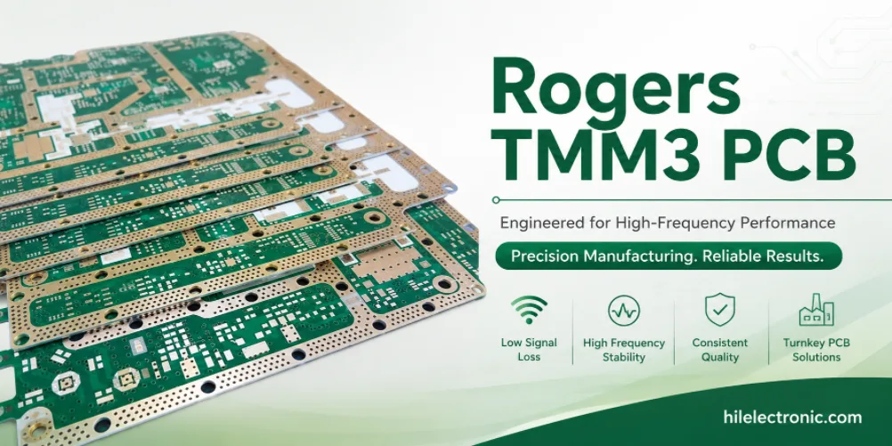
Rogers TMM3 PCB Manufacturer for Mechanical RF Modules
TMM3 is selected when an RF circuit must behave as part of...
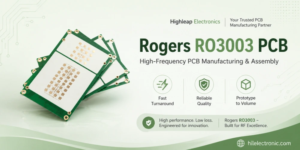
Rogers RO3003 PCB Manufacturer for Automotive Radar and mmWave Modules
A 77 GHz radar board is purchased as a working sensor...
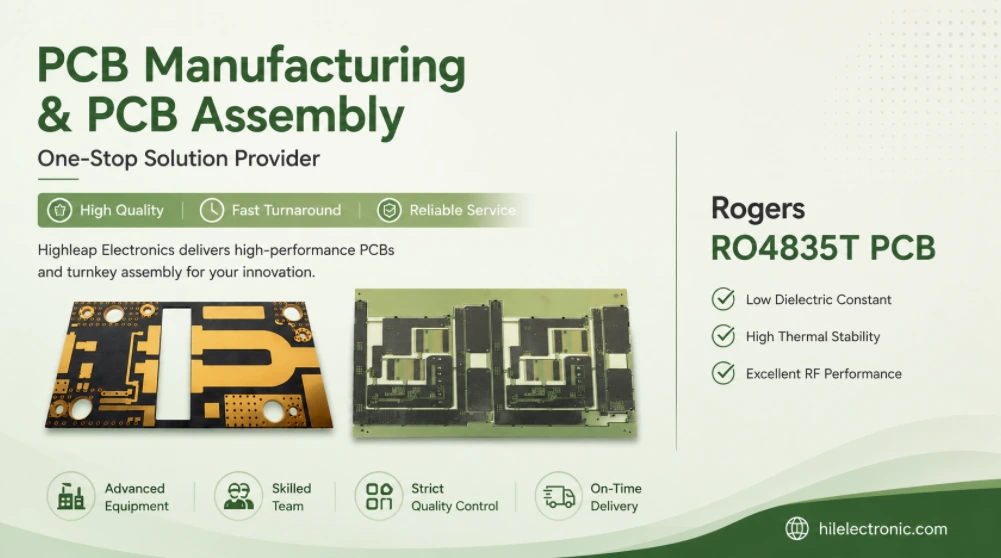
Rogers RO4835T PCB Manufacturer for Thin-Core RF Multilayer Boards
RO4835T is useful when the RF layer must move inside the...
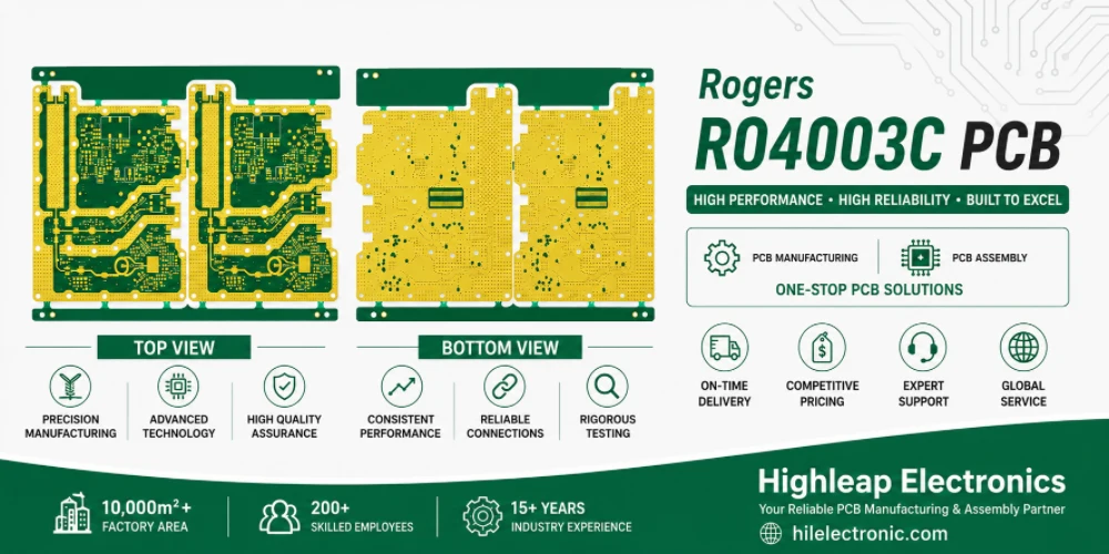
Rogers RO4003C PCB Manufacturer for RF and Hybrid Multilayer Boards
RO4003C is often the point where an RF project stops...
How to get a quote for PCBs
Let us run DFM/DFA analysis for you and get back to you with a report.
You can upload your files securely through our website.
We require the following information in order to give you a quote:
-
- Gerber, ODB++, or .pcb, spec.
- BOM list if you require assembly
- Quantity
- Turn time
In addition to PCB manufacturing, we offer a comprehensive range of electronic services, including PCB design, PCBA (Printed Circuit Board Assembly), and turnkey solutions. Whether you need help with prototyping, design verification, component sourcing, or mass production, we provide end-to-end support to ensure your project’s success. For PCBA services, please provide your BOM (Bill of Materials) and any specific assembly instructions. We also offer DFM/DFA analysis to optimize your designs for manufacturability and assembly, ensuring a smooth production process.