
Ceramic PCB Manufacturing Company for Volume Production

Table of Contents
- Why Ceramic PCB Projects Stall Between Prototype and Production
- Phase 1: Prototype — Validating Design and Material Choices
- Phase 2: Engineering Pilot — Qualifying the Production Process
- Phase 3: Production Ramp — Scaling Without Quality Drift
- Cost Engineering: Reducing Ceramic PCB Unit Cost at Volume
- Choosing a Manufacturing Company That Supports the Full Lifecycle
Getting a ceramic PCB prototype to work on the bench is one thing. Getting 5,000 identical boards delivered on schedule, at target cost, with consistent quality — that is an entirely different engineering challenge. And it is where most ceramic PCB projects run into trouble.
The gap between prototype and volume production is where material inconsistencies surface, where process yields become critical, and where the relationship with your ceramic PCB manufacturing company either accelerates your timeline or becomes a bottleneck.
This guide covers the practical steps for transitioning a ceramic PCB project from prototype through pilot to volume — with specific attention to the process qualifications, cost optimizations, and supplier coordination that make the difference between a smooth ramp and a painful one.
1. Why Ceramic PCB Projects Stall Between Prototype and Production
1.1 Common Failure Modes
Based on typical project patterns, the most frequent causes of prototype-to-production delays for ceramic PCBs include:
- Material specification gaps: The prototype used a specific substrate lot with above-average thermal conductivity; the production lot falls within spec but performs differently enough to affect thermal margins
- Process yield surprises: A metallization process that worked at 90% yield for 20 prototype pieces drops to 70% yield at 500-piece volume because process parameters were not formally qualified
- Supplier handoff friction: The prototype was built at a lab or specialty house that cannot scale; the production supplier needs to re-develop the process from scratch
- Test coverage gaps: Prototype testing validated electrical function but not reliability — and early production boards fail thermal cycling in the field
- Cost surprises: Prototype unit cost was acceptable at small volume; production quotes come in 2–3× higher than budgeted because of material waste, yield losses, or test complexity
1.2 The Root Cause
Most of these problems share a common root: the prototype phase did not include the production supplier, so the knowledge gained during prototyping did not transfer to the production process. The most efficient approach is to engage your ceramic PCB manufacturing company from the prototype stage — so prototype learning directly informs production process development.

2. Phase 1: Prototype — Validating Design and Material Choices
2.1 Objectives
The prototype phase should validate three things:
- The chosen ceramic material delivers the required thermal and electrical performance
- The metallization method produces reliable adhesion and the required pattern resolution
- The assembled board passes functional and reliability screening tests
2.2 What to Specify in Your Prototype Order
| Item | Prototype Phase Requirement |
|---|---|
| Quantity | 10–30 pieces (enough for assembly validation + destructive testing) |
| Material | Same grade intended for production (do not prototype on premium material if production uses standard grade) |
| Metallization | Same method as production (do not prototype with thin film if production will use thick film) |
| Testing | Include at least 5 boards for reliability screening (thermal shock, adhesion, dielectric) |
| Documentation | Request process parameter records — these become the baseline for production qualification |
Highleap supports ceramic PCB prototyping through our rapid prototyping services, with typical turnaround of 7–12 business days including DFM review and engineering feedback.
2.3 DFM Review: Catching Production Problems Early
A critical step that many teams skip during prototyping is DFM review for production scalability. Your manufacturing partner should flag issues such as:
- Via placements that risk ceramic cracking at production-speed laser drilling
- Trace geometries that are achievable but yield-sensitive at volume
- Panelization layouts that waste substrate material or complicate singulation
- Surface finish selections that require additional process steps not justified by the application
Our ceramic PCB fabrication team performs DFM review on every prototype order, providing specific, actionable feedback — not generic checklists.
3. Phase 2: Engineering Pilot — Qualifying the Production Process
3.1 Purpose
The engineering pilot run (typically 50–200 pieces) serves to qualify the production process — confirming that the process parameters established during prototyping produce conforming boards consistently when run at production speed and volume.
3.2 Process Qualification Activities
- Process capability study (Cpk): Measure critical dimensions across the pilot lot to verify statistical capability — Cpk ≥1.33 for critical parameters, Cpk ≥1.0 for standard parameters
- First Article Inspection (FAI): Complete dimensional and electrical characterization of initial production boards against drawing specifications
- Reliability qualification: Submit pilot boards to the full PCB reliability test suite — thermal shock, humidity exposure, dielectric breakdown — to validate production boards meet the same reliability as prototypes
- Assembly process validation: If turnkey assembly is included, qualify reflow profiles, wire bonding parameters, and inspection criteria during the pilot run
3.3 Documentation Deliverables from Pilot
At the end of the pilot phase, your manufacturing partner should provide:
- ☐ First Article Inspection report
- ☐ Process capability data (Cpk) for critical dimensions
- ☐ Reliability test results (thermal shock, adhesion, dielectric)
- ☐ Yield data with root cause analysis for any rejects
- ☐ Finalized process control plan for volume production

4. Phase 3: Production Ramp — Scaling Without Quality Drift
4.1 The Scaling Challenge
Ceramic PCB processes are less forgiving of variation than FR4 processes. A 2°C drift in DBC bonding temperature that causes no issue at prototype scale can produce measurable adhesion degradation across a 1,000-piece production lot. Effective production ramp management requires:
- Equipment monitoring: Continuous logging of furnace temperature, atmosphere composition, and cooling rate during every production run
- Lot-level traceability: Every finished board traceable to its raw substrate lot, metallization run, and inspection data
- SPC with real-time alerting: Critical parameters monitored against control limits, with production automatically paused if parameters drift outside tolerance
4.2 Ongoing Quality Assurance
Production-phase quality assurance extends beyond in-process inspection:
- Periodic reliability sampling (e.g., 5 boards per 500-piece lot submitted to thermal shock testing)
- X-ray inspection of assembled boards for hidden joint defects
- Cross-section analysis on a statistical basis to verify copper thickness and metallization integrity
- Customer-specified functional testing on every unit (if applicable)
5. Cost Engineering: Reducing Ceramic PCB Unit Cost at Volume
5.1 Legitimate Cost Reduction Strategies
As production volume increases, a well-managed ceramic PCB manufacturing company can identify cost reduction opportunities without compromising quality:
| Strategy | Typical Saving | Engineering Requirement |
|---|---|---|
| Panelization optimization | 10–20% material cost reduction | Redesign panel layout for maximum substrate utilization |
| Material grade rationalization | 15–30% substrate cost reduction | Verify that 96% alumina meets requirements (vs. specifying 99.6% by default) |
| Yield improvement | 5–15% total cost reduction | Process optimization based on pilot run data |
| Test optimization | 5–10% per-unit test cost | Reduce sampling rate once process Cpk is demonstrated |
| Supply chain consolidation | 10–15% logistics and overhead | Use integrated component sourcing to combine fab + parts + assembly in one PO |
5.2 Cost Traps to Avoid
- Switching to a cheaper substrate supplier mid-production without re-qualifying the metallization process
- Reducing inspection sampling before process capability is proven
- Eliminating reliability testing to save per-unit cost — this shifts risk from the factory to the field
- Splitting fabrication and assembly across different vendors to save apparent cost, while increasing total cost through logistics, handling damage, and coordination overhead
6. Choosing a Manufacturing Company That Supports the Full Lifecycle
The most efficient path from ceramic PCB prototype to volume production is working with a single manufacturing partner from the start. This means your prototype process data feeds directly into production qualification, DFM improvements compound across iterations, and there is no knowledge loss during supplier transitions.
Highleap Electronics supports this lifecycle approach through:
- Prototype: Rapid ceramic PCB fabrication (7–12 days) with DFM review and engineering feedback
- Pilot: Engineering pilot runs with FAI, Cpk analysis, and reliability testing
- Production: Volume manufacturing with SPC monitoring, lot traceability, and thermal performance validation
- Assembly: SMT assembly services, wire bonding, die attach, and final testing under one roof
- Ongoing support: Cost engineering, yield improvement, and design iteration support throughout the product lifecycle
Our multi-certification quality system (ISO 9001 + ISO 13485 + IATF 16949 + ISO 14001) provides the documentation infrastructure required for automotive, medical, industrial, and consumer electronics applications.
Start Your Ceramic PCB Project
Ready to move from design to qualified production? Send us your files and specifications — we will map out the prototype-to-volume plan for your project.
Shirley has 5 years of hands-on experience in PCB fabrication and assembly services. Her expertise includes complex multilayer boards, HDI structures, turnkey component sourcing, SMT assembly, testing, and full system integration. As both a technical advisor and sales specialist, she supports customers with DFM guidance, cost optimization, and production planning, helping projects move efficiently from design to mass production with consistent quality and on-time delivery.

Recommended Posts
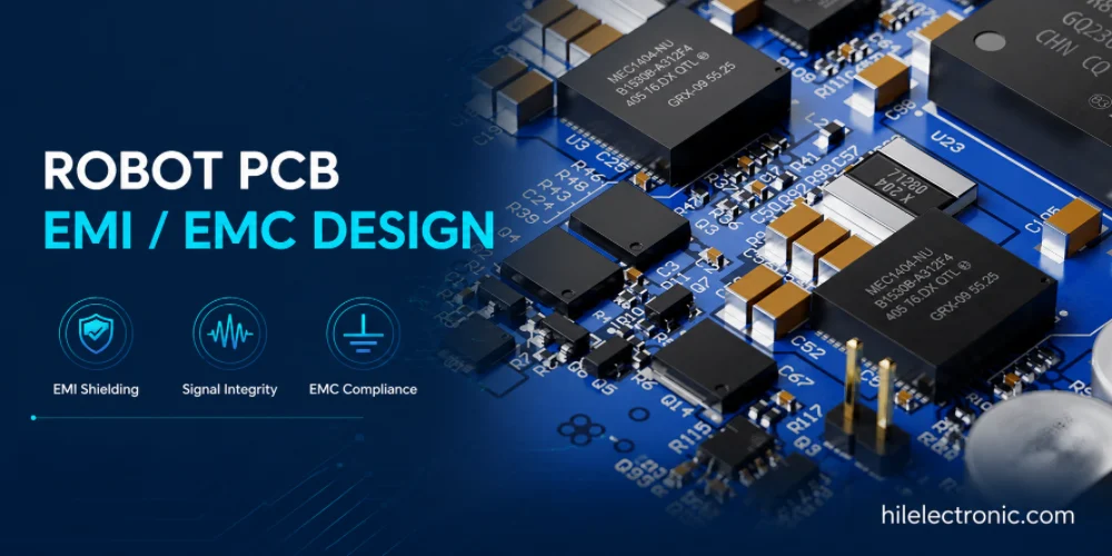
Robot PCB EMI/EMC Design for Reliable Robotics
Robot PCB EMI and EMC design affects whether a robot can...
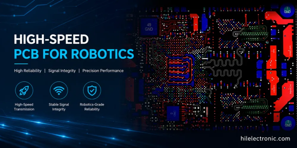
High-Speed PCB for Robotics: PCIe, DDR, MIPI and Ethernet Layout
High-speed PCB manufacturing for robotics supports data...
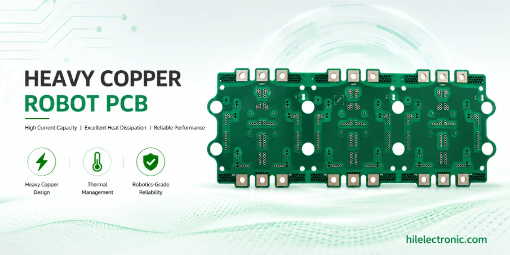
Heavy Copper Robot PCB for Motor Drives, BMS and Power Distribution
Heavy copper robot PCBs are used when standard 1 oz copper...

Rigid-Flex PCB for Robotics: Joint Interconnects That Survive Motion
Rigid-flex PCB manufacturing for robotics is valuable when...
How to get a quote for PCBs
Let us run DFM/DFA analysis for you and get back to you with a report.
You can upload your files securely through our website.
We require the following information in order to give you a quote:
-
- Gerber, ODB++, or .pcb, spec.
- BOM list if you require assembly
- Quantity
- Turn time
In addition to PCB manufacturing, we offer a comprehensive range of electronic services, including PCB design, PCBA (Printed Circuit Board Assembly), and turnkey solutions. Whether you need help with prototyping, design verification, component sourcing, or mass production, we provide end-to-end support to ensure your project’s success. For PCBA services, please provide your BOM (Bill of Materials) and any specific assembly instructions. We also offer DFM/DFA analysis to optimize your designs for manufacturability and assembly, ensuring a smooth production process.