
Ceramic PCB Fabrication Services Focused on Board Quality

Table of Contents
- What Makes Ceramic PCB Fabrication Different from Standard PCB Manufacturing
- Fabrication Process: Step by Step
- Material Options and How They Affect Process Routing
- Critical Process Parameters That Determine Board Quality
- Surface Finishing and Post-Processing
- How to Prepare Your Design Files for Ceramic Fabrication
- Highleap’s Ceramic PCB Fabrication Services
Ceramic PCB fabrication services follow a fundamentally different process from FR4 board manufacturing. While FR4 production involves laminating copper foil to pre-made resin-glass substrates, ceramic fabrication starts with raw ceramic substrates that require sintering at temperatures exceeding 1,500°C, followed by metallization processes that bond conductive layers to the ceramic surface through chemical or mechanical means.
This difference means that not every PCB factory can produce ceramic boards — even if they list it on their website. Understanding what is actually involved in the fabrication process helps engineers specify their requirements correctly and evaluate whether a ceramic PCB fabrication provider has the real capability to deliver.
1. What Makes Ceramic PCB Fabrication Different from Standard PCB Manufacturing
1.1 Process Temperature
FR4 PCBs are processed below 200°C for lamination and 260°C for reflow soldering. Ceramic substrates, by contrast, are sintered at 850–1,700°C depending on the material and process type. This requires specialized high-temperature furnaces with precise atmosphere control — equipment that standard PCB factories simply do not have.
1.2 Material Behavior
Ceramic is brittle. Unlike FR4, which can be drilled, routed, and handled with standard mechanical processes, ceramic substrates require laser drilling for vias, diamond scribing or laser cutting for singulation, and careful handling throughout production to prevent cracking. A single mishandled panel can scrap an entire production lot.
1.3 Metallization Chemistry
Copper does not naturally adhere to ceramic. Creating a reliable conductor layer requires specialized bonding processes — DBC (Direct Bonded Copper), thick-film screen printing, thin-film sputtering, or AMB (Active Metal Brazing) — each with different equipment, materials, and process parameters. The metallization method determines the achievable trace resolution, current-carrying capacity, and long-term reliability of the finished board.

2. Fabrication Process: Step by Step
2.1 Overview
A typical ceramic PCB fabrication sequence includes:
- Substrate preparation: Incoming inspection of raw ceramic blanks (purity, dimensions, surface roughness), followed by cleaning and lapping to the required surface profile
- Metallization: Applying the conductive layer through DBC bonding, thick-film printing and firing, thin-film deposition, or AMB process
- Circuit patterning: Photolithography and etching to define trace geometry from the metallized surface
- Via formation: Laser drilling through the ceramic substrate; via filling with conductive paste or plating
- Surface finishing: ENIG, hard gold, Ni/Ag, or OSP — selected based on assembly method and application
- Singulation: Laser scribing, diamond cutting, or snap-apart scoring to separate individual boards from the production panel
- Inspection and testing: Dimensional verification, electrical continuity/isolation testing, visual inspection, and reliability testing as specified
2.2 Process Variations by Metallization Method
| Method | Temperature | Min. Trace Width | Cu Thickness | Best For |
|---|---|---|---|---|
| DBC | ~1,065°C | 0.15 mm | 0.15–0.6 mm | Power electronics, IGBT modules |
| Thick film | 850–1,000°C | 0.30 mm | 10–25 µm (paste) | Hybrid circuits, sensors, LED |
| Thin film | Room temp (sputtering) | 0.025 mm | 2–10 µm | RF/microwave, fine-line circuits |
| AMB | 800–900°C | 0.20 mm | 0.2–0.8 mm | Si₃N₄ substrates, high-reliability power |
For an in-depth look at DBC-specific fabrication, see our DBC substrate manufacturing guide.
3. Material Options and How They Affect Process Routing
The ceramic substrate material determines not just the board’s thermal and electrical performance, but also which fabrication processes can be used:
| Material | Thermal Cond. (W/m·K) | Compatible Metallization | Key Limitation |
|---|---|---|---|
| Al₂O₃ 96% | 24–28 | DBC, thick film, thin film | Moderate thermal performance |
| Al₂O₃ 99.6% | 30–33 | DBC, thick film, thin film | Higher cost than 96% grade |
| AlN | 170–230 | DBC, AMB, thin film | Moisture sensitivity; requires controlled storage |
| Si₃N₄ | 70–90 | AMB (preferred), DBC | Highest mechanical strength; difficult to process |
For detailed material comparison and selection guidance, our alumina PCB manufacturing guide covers the most widely used ceramic substrate option.
4. Critical Process Parameters That Determine Board Quality
4.1 Sintering / Bonding Temperature Control
DBC bonding requires furnace temperature uniformity within ±3–5°C across the entire hot zone. Even small temperature gradients cause uneven copper-ceramic bond strength — strong in the center, weak at the edges — leading to delamination failures under thermal cycling.
4.2 Atmosphere Control
Both DBC bonding and thick-film firing require precise atmosphere management. DBC bonding uses nitrogen with controlled trace oxygen (typically 10–50 ppm O₂) to form the copper oxide interface that enables bonding. Too much oxygen produces excessive oxidation; too little prevents bond formation. Thick-film firing uses nitrogen to prevent conductor oxidation during sintering.
4.3 Dimensional Control
Ceramic substrates shrink during sintering — typically 15–20% depending on the material and process. This shrinkage must be compensated in the green-tape design (for LTCC/HTCC) or controlled through substrate selection tolerances for post-fired metallization processes. Final dimensional tolerance for production ceramic PCBs is typically ±0.05–0.10 mm.
4.4 Peel Strength
The adhesion between conductor and ceramic — measured by 90° peel test per IPC-TM-650 — is the most critical quality metric for ceramic PCB reliability. Well-controlled DBC achieves >8 N/mm; marginal processes deliver 4–5 N/mm. Specify minimum acceptance criteria in your purchase order.

5. Surface Finishing and Post-Processing
Surface finish selection depends on the downstream assembly process:
- ENIG (Electroless Nickel / Immersion Gold): Standard for SMT assembly; provides flat, solderable surface with good shelf life. Ni: 3–6 µm, Au: 0.05–0.1 µm
- Hard gold (electrolytic): Required for wire bonding (Au or Al wire) and high-wear contact areas. Au: 0.5–2.5 µm over Ni barrier
- Ni/Ag: Common for power module soldering; provides excellent solderability and lower cost than gold finishes
- OSP: Economical option for designs that will be assembled shortly after fabrication; limited shelf life
Post-processing steps may include laser trimming of resistor values (for thick-film circuits), cavity milling for component recessing, and edge chamfering to reduce chipping risk during handling.
6. How to Prepare Your Design Files for Ceramic Fabrication
Ceramic PCB fabrication requires more complete documentation than standard FR4 orders. Your file package should include:
- ☐ Gerber files (copper layers, solder mask, silkscreen, substrate outline, stiffener/cavity layers if applicable)
- ☐ Fabrication drawing with complete dimensioning, tolerances, material callout, and surface finish specification
- ☐ Stackup specification (substrate material, thickness, metallization method, copper thickness)
- ☐ Electrical test requirements (continuity, isolation resistance values)
- ☐ Reliability test requirements (thermal shock cycles, peel strength minimum, dielectric withstand voltage)
- ☐ Panelization preferences (or allow the manufacturer to optimize)
Missing or ambiguous specifications are the single largest source of quality problems in ceramic PCB fabrication. Invest time in documentation upfront — it saves weeks of back-and-forth and potential re-builds.
7. Highleap’s Ceramic PCB Fabrication Services
Highleap Electronics operates dedicated ceramic PCB fabrication lines in Guangzhou, China, supporting the full range of substrate materials and metallization processes:
- Materials: Al₂O₃ (96%, 99.6%), AlN, Si₃N₄ — with incoming inspection and lot traceability for every substrate
- Metallization: DBC (Cu 0.15–0.6 mm), thick film (Ag-Pd, Au), thin film (sputtered Cu/Au), AMB
- Tolerances: ±0.05 mm dimensional accuracy; laser via capability down to 0.1 mm diameter
- Surface finishes: ENIG, hard gold, Ni/Ag, OSP
- Quality system: ISO 9001 + ISO 13485 + IATF 16949 + ISO 14001
- DFM support: Free engineering review on every order with specific, actionable feedback
We provide fabrication-only services for teams that handle assembly separately, as well as integrated fabrication + PCB assembly for those who prefer a single-vendor solution. Our thermal management engineering team is available to help optimize substrate selection and thermal via strategies before your design goes to production.
Sabrina has over 18 years of experience in the PCB industry, with a strong background in CAM engineering and PCB file review. She supports PCB projects from prototype to volume production, focusing on manufacturability and process reliability. Her work helps engineering teams reduce production risk and achieve stable, high-quality PCB manufacturing results.

Recommended Posts
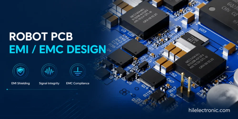
Robot PCB EMI/EMC Design for Reliable Robotics
Robot PCB EMI and EMC design affects whether a robot can...
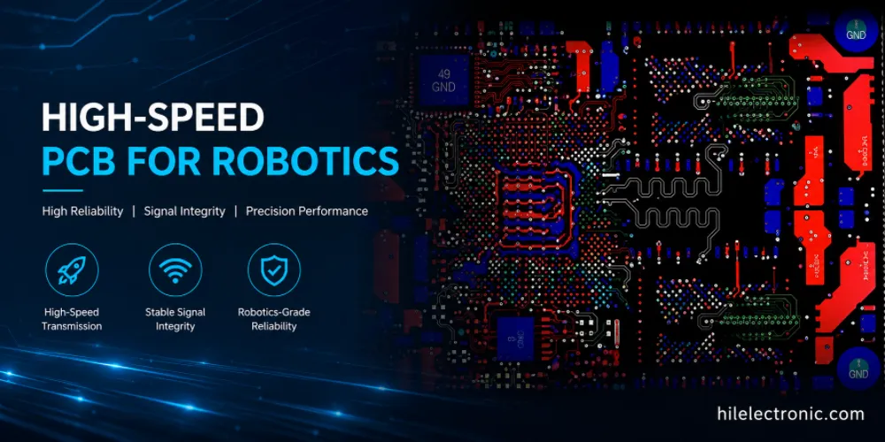
High-Speed PCB for Robotics: PCIe, DDR, MIPI and Ethernet Layout
High-speed PCB manufacturing for robotics supports data...
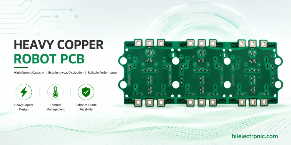
Heavy Copper Robot PCB for Motor Drives, BMS and Power Distribution
Heavy copper robot PCBs are used when standard 1 oz copper...

Rigid-Flex PCB for Robotics: Joint Interconnects That Survive Motion
Rigid-flex PCB manufacturing for robotics is valuable when...
How to get a quote for PCBs
Let us run DFM/DFA analysis for you and get back to you with a report.
You can upload your files securely through our website.
We require the following information in order to give you a quote:
-
- Gerber, ODB++, or .pcb, spec.
- BOM list if you require assembly
- Quantity
- Turn time
In addition to PCB manufacturing, we offer a comprehensive range of electronic services, including PCB design, PCBA (Printed Circuit Board Assembly), and turnkey solutions. Whether you need help with prototyping, design verification, component sourcing, or mass production, we provide end-to-end support to ensure your project’s success. For PCBA services, please provide your BOM (Bill of Materials) and any specific assembly instructions. We also offer DFM/DFA analysis to optimize your designs for manufacturability and assembly, ensuring a smooth production process.