
Ceramic PCB Manufacturer in China

Table of Contents
- Ceramic PCB Manufacturing in China: Current Landscape
- Core Manufacturing Capabilities to Evaluate
- Material Processing and Substrate Handling
- Metallization Technology and Process Control
- Testing, Inspection, and Reliability Validation
- Integrated Assembly: Why It Matters for Ceramic Boards
- Highleap Electronics: Manufacturing Capabilities Overview
When engineers evaluate a ceramic PCB manufacturer in China, the conversation usually starts with price and lead time. But for ceramic substrates — where sintering temperatures exceed 1,500°C, metallization adhesion depends on atmosphere-controlled bonding, and a 0.1 mm dimensional error can cause thermal failure — manufacturing capability is what actually determines whether your boards will work in the field.
This article breaks down the specific technical capabilities that separate a qualified ceramic PCB manufacturer from a general-purpose PCB factory that happens to list ceramic in its product catalog.
1) Ceramic PCB Manufacturing in China: Current Landscape
1.1 Market Segmentation
China’s ceramic PCB manufacturing sector broadly falls into three tiers:
| Tier | Characteristics | Typical Customers |
|---|---|---|
| Tier 1: Specialist ceramic factories | Dedicated ceramic lines, in-house sintering and metallization, multiple material capability (Al₂O₃, AlN, Si₃N₄) | Automotive OEMs, power semiconductor companies, medical device manufacturers |
| Tier 2: Mixed-capability factories | Primarily FR4/metal-core production with ceramic as a secondary offering; often outsource sintering or metallization | LED manufacturers, general industrial electronics |
| Tier 3: Trading companies / brokers | No in-house ceramic capability; subcontract everything and add margin | Low-volume, cost-sensitive projects with relaxed quality requirements |
For power electronics, RF/microwave, and medical applications, Tier 1 is the only viable option. The risk of quality issues, communication gaps, and supply chain opacity increases dramatically with Tier 2 and Tier 3 suppliers.
1.2 Regional Concentration
Most qualified ceramic PCB production in China is concentrated in the Pearl River Delta (Guangdong province) and the Yangtze River Delta (Jiangsu/Zhejiang). These regions offer proximity to ceramic raw material suppliers, skilled labor pools with ceramic processing experience, and established logistics infrastructure for international shipping.
2) Core Manufacturing Capabilities to Evaluate
2.1 Capability Matrix
Use this matrix to benchmark Chinese ceramic PCB factories during your evaluation:
| Capability | Must-Have | Preferred |
|---|---|---|
| Ceramic materials processed | Al₂O₃ (96% and 99.6%) | + AlN, Si₃N₄ |
| Metallization methods | At least one of DBC / thick film / thin film | Multiple methods in-house |
| Minimum trace width | 0.30 mm (thick film); 0.15 mm (DBC) | 0.10 mm (thin film) |
| Laser via capability | 0.15 mm diameter | 0.10 mm diameter |
| Dimensional tolerance | ±0.10 mm | ±0.05 mm |
| In-house assembly | SMT capability | + Wire bonding, die attach |
| Certifications | ISO 9001 | + IATF 16949, ISO 13485 |
2.2 What the Datasheet Does Not Tell You
Quoted specs on a website do not equal demonstrated production capability. Ask for:
- Production records from the last 6 months showing actual achieved tolerances
- Yield rate data for projects similar to yours in material, complexity, and volume
- Cross-section photographs of DBC bonds or thick-film metallization from recent lots
- Customer references in your industry segment (with permission to contact)
3) Material Processing and Substrate Handling
3.1 Incoming Material Control
A serious ceramic PCB manufacturing operation controls quality from the moment raw substrates arrive. This means incoming inspection that verifies purity (e.g., XRF analysis confirming Al₂O₃ content), dimensional measurement of substrate blanks, surface roughness profiling, and visual inspection for pre-existing cracks or inclusions.
Factories that skip incoming inspection and assume their substrate suppliers always deliver conforming material will eventually pass defective substrates into production — and the defect will surface as a field failure, not a manufacturing reject.
3.2 Substrate Preparation
Before metallization, ceramic substrates require precise surface preparation:
- Cleaning: Ultrasonic cleaning in solvent baths removes organic contaminants that prevent metallization adhesion
- Lapping/polishing: Surface roughness must be controlled to match the metallization method — DBC requires a different surface profile than thin film
- Edge processing: Laser cutting or diamond scribing defines substrate boundaries with minimal chipping
For alumina substrate fabrication, the difference between 96% and 99.6% purity grades affects both lapping parameters and achievable surface roughness, which in turn impacts metallization quality.
4) Metallization Technology and Process Control
4.1 DBC (Direct Bonded Copper)
DBC bonding is the most demanding metallization process. The copper-ceramic interface forms at approximately 1,065°C under precisely controlled atmosphere (typically nitrogen with trace oxygen). Critical process parameters include:
- Temperature uniformity across the furnace hot zone: ±3–5°C
- Oxygen partial pressure control during bonding
- Cooling rate management to minimize residual stress
- Post-bond etching precision for copper circuit patterning
Factories with well-controlled DBC processes achieve peel strengths above 8 N/mm consistently. Those with marginal control hover around 4–5 N/mm and show higher lot-to-lot variation. Our DBC substrate technical overview explains the bonding mechanism and quality criteria in detail.
4.2 Thick Film
Thick film ceramic PCB processing involves screen-printing conductive pastes and sintering at 850–1,000°C. Process control centers on:
- Screen mesh quality and tension (200–400 mesh for standard resolution)
- Paste viscosity and print thickness uniformity
- Firing profile control (peak temperature, dwell time, cooling rate)
- Registration accuracy between print layers
4.3 Process Documentation Standards
Regardless of metallization method, a qualified manufacturer maintains process flow documentation for each material/method combination, statistical process control (SPC) charts for critical parameters, and operator qualification records for specialized equipment. Without these, process consistency depends on individual operator skill rather than systematic control — and that does not scale.
5) Testing, Inspection, and Reliability Validation
5.1 In-Process Inspection
Effective quality control for ceramic PCBs requires inspection at every major process stage — not just final outgoing QC:
- Post-sintering: Dimensional check, visual inspection for cracks, flatness measurement
- Post-metallization: Copper thickness verification, adhesion testing (peel or pull test), electrical continuity
- Post-patterning: Trace width/space measurement, isolation resistance testing
- Post-assembly: X-ray inspection for BGA/QFN joints, AOI for SMT placement accuracy
5.2 Reliability Testing
For ceramic PCBs destined for power electronics, automotive, or aerospace applications, reliability testing is not optional:
- Thermal shock: –40°C to +150°C cycling, typically 100–500 cycles
- Power cycling: Simulates real-world load conditions for DBC-based power modules
- Dielectric breakdown: Verifies insulation integrity under high-voltage stress
- Moisture resistance: 85°C / 85% RH exposure for 168–1,000 hours
A manufacturer that cannot provide reliability test data from their production is asking you to do their qualification testing at your expense — and at the risk of your product schedule.
6) Integrated Assembly: Why It Matters for Ceramic Boards
Ceramic PCBs frequently require assembly processes that differ from standard FR4 boards:
- High-temperature reflow profiles must be optimized for ceramic thermal mass to prevent cracking
- Wire bonding for die-attach applications requires gold or aluminum wedge bonding capability
- Handling procedures must account for ceramic brittleness — automated pick-and-place systems need adapted vacuum nozzles and placement force limits
A ceramic PCB manufacturer in China that also provides in-house PCB assembly eliminates the risk of substrate damage during transit between separate fab and assembly vendors. It also enables process optimization across the full build — adjusting reflow profiles based on substrate thermal characteristics, for example, rather than using generic profiles designed for FR4.
For DBC substrate-based power modules, integrated assembly is particularly important because the die-attach process must be tightly coordinated with substrate surface metallization quality.
7) Highleap Electronics: Manufacturing Capabilities Overview
Highleap Electronics operates an integrated PCB manufacturing and assembly facility in Guangzhou, China, with dedicated ceramic PCB production lines. Our ceramic PCB technology capabilities include:
- Materials: Al₂O₃ (96%, 99.6%), AlN, Si₃N₄ — with incoming inspection and lot traceability
- Metallization: DBC (Cu thickness 0.15–0.6 mm) and thick film (Ag-Pd, Au) with ±0.05 mm dimensional control
- Laser processing: Via drilling down to 0.1 mm; laser scribing for substrate singulation
- Assembly: 5 SMT lines, wire bonding, die attach, conformal coating, functional testing
- Certifications: ISO 9001, ISO 13485, ISO 14001, IATF 16949
- Engineering support: Bilingual team providing DFM review, material selection guidance, and thermal management optimization
We serve customers in power electronics, automotive, LED lighting, medical devices, and RF/microwave — industries where ceramic substrate quality directly impacts product reliability and field performance.
Send us your project specifications and we will provide a detailed assessment of how our ceramic PCB manufacturing capabilities match your requirements.
Shirley has 5 years of hands-on experience in PCB fabrication and assembly services. Her expertise includes complex multilayer boards, HDI structures, turnkey component sourcing, SMT assembly, testing, and full system integration. As both a technical advisor and sales specialist, she supports customers with DFM guidance, cost optimization, and production planning, helping projects move efficiently from design to mass production with consistent quality and on-time delivery.

Recommended Posts
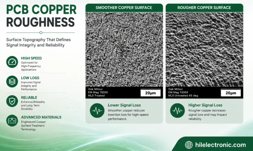
PCB Copper Roughness: Signal Loss, Material Selection and Manufacturing Control
Table of contentsWhat Is PCB Copper Roughness?How Copper...
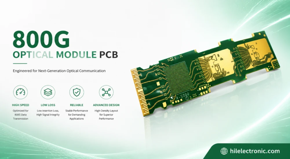
800G Optical Module PCB Manufacturing and Assembly Service
Table of contentsWhat Makes an 800G Optical Module PCB...
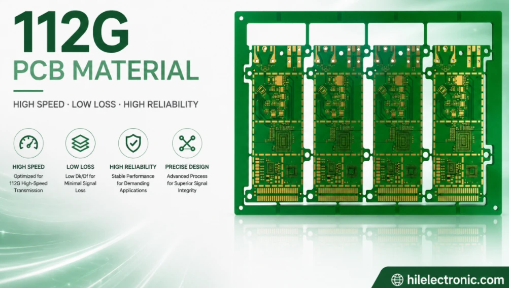
112G PCB Material Selection and High-Speed PCB Manufacturing
Table of contentsWhat “112G PCB Material” Actually...
77 GHz Radar PCB Material Selection and Manufacturing Guide
Table of contentsWhat 77 GHz Changes in a PCBCommon 77 GHz...
How to get a quote for PCBs
Let us run DFM/DFA analysis for you and get back to you with a report.
You can upload your files securely through our website.
We require the following information in order to give you a quote:
-
- Gerber, ODB++, or .pcb, spec.
- BOM list if you require assembly
- Quantity
- Turn time
In addition to PCB manufacturing, we offer a comprehensive range of electronic services, including PCB design, PCBA (Printed Circuit Board Assembly), and turnkey solutions. Whether you need help with prototyping, design verification, component sourcing, or mass production, we provide end-to-end support to ensure your project’s success. For PCBA services, please provide your BOM (Bill of Materials) and any specific assembly instructions. We also offer DFM/DFA analysis to optimize your designs for manufacturability and assembly, ensuring a smooth production process.