
Back to blog
Overview of PCB Assembly Manufacturing Processes and Technologies

PCB Assembly Manufacturing is a complex process involving various steps, each critical to the functionality of electronic devices. This article provides a detailed overview of each step in the PCBA process, introducing the technologies and techniques employed at every stage.
1. Solder Paste Stenciling
This is the first step where solder paste is applied to the board. A stencil is used to apply the paste only on the parts where components will be mounted.
- Stencil Printer: Ensures precise application of solder paste.
- Laser-Cut Stencils: Provide accuracy and fine detail in solder paste application.
2. Pick and Place
Electronic components are placed on the PCB. This step requires precision as components must align with the solder paste.
- Automated Pick and Place Machines:These machines are the heart of the Pick and Place process. They use vacuum nozzles to pick up individual components from the feeders and precisely place them on their designated spots on the PCB.The latest machines are equipped with high-speed robotics, capable of placing thousands of components per hour with exceptional precision.Optical Positioning
- Systems:Advanced cameras and optical systems are integrated into the machines for accurate component placement.
These systems ensure that components, some of which can be extremely small (like 0201 or 01005 sizes), are accurately positioned. - Component Feeders:Components are supplied to the pick and place machines via feeders.These can be reel feeders for tape-and-reel components, tray feeders for bulk components, or tube feeders for certain types of ICs.
- Programming and Software:The machines are programmed with the PCB design data, which directs the placement of each component.Software is used to optimize the placement sequence, reducing the time taken and enhancing efficiency.
- Quality Control:Post-placement inspection is often conducted to verify the accuracy of component placement.Some systems incorporate real-time monitoring and adjustments during the placement process.

3. Reflow Soldering
After placement, the board passes through a reflow oven where the solder paste melts and solidifies, forming a solid solder joint between the components and the board.
- Conveyor Reflow Ovens: Provide controlled heating and cooling cycles.
- Temperature Profiling: Ensures optimal heating for different types of components and solder.
- Preheating Phase:Before reaching the melting point of the solder paste, the PCB assembly undergoes a preheating or “soak” phase.This stage gradually heats the PCB to prevent component shock and evaporates any solvents in the solder paste.
- Thermal Profiling:The entire process follows a thermal profile, which is a precise control of temperature over time.Proper thermal profiling is crucial to ensure optimal flow of the solder, minimize defects, and manage the thermal stress on components.
- Reflow Phase:In this phase, the temperature is raised above the solder’s melting point, causing it to liquefy and bond the component leads or pads to the PCB.The surface tension of the molten solder helps keep components in place and forms reliable solder joints.
- Cooling Phase:After reflow, the assembly is cooled in a controlled manner to solidify the solder.Controlled cooling is vital to prevent thermal shock and ensure the formation of sound solder joints with good mechanical and electrical properties.
4. PCB Assembly Manufacturing Inspection and Quality Control
After the soldering process in PCB assembly manufacturing, rigorous inspection and quality control measures are essential to ensure the integrity and functionality of the boards. Here’s a detailed look into the inspection processes commonly employed:
Automatic Optical Inspection (AOI)
Automatic Optical Inspection (AOI) utilizes high-resolution cameras and advanced algorithms to scrutinize the surface of assembled PCBs. This technology is pivotal in detecting various surface defects that could compromise the board’s performance or reliability. AOI checks for:
- Solder Joint Quality: AOI identifies issues such as solder bridges (short circuits between adjacent pads), insufficient solder, or solder voids that could affect electrical connections.
- Component Placement Accuracy: It verifies the correct placement of components according to the design specifications, ensuring alignment and orientation are precise.
- Surface Mount Device (SMD) Defects: AOI inspects SMD components for orientation, polarity, and presence, ensuring all components are correctly mounted.
X-Ray Inspection
X-Ray Inspection is indispensable for inspecting the integrity of solder joints and connections that are not visible to the naked eye. This non-destructive testing method provides insights into:
- Underfill Inspection: X-Ray technology detects voids or cracks in underfill materials used to secure components, ensuring they adhere properly without compromising structural integrity.
- BGA (Ball Grid Array) Inspection: It examines the solder balls beneath BGA components to verify soldering quality, ensuring each ball is properly soldered to its corresponding pad.
3D Solder Paste Inspection (SPI)
3D Solder Paste Inspection (SPI) measures and validates the volume and placement accuracy of solder paste deposited on PCBs before component placement. This inspection process involves:
- Volume Verification: SPI precisely measures the volume of solder paste deposited on each pad, ensuring consistency and adequacy for reliable solder joints.
- Placement Accuracy: It verifies the precise positioning of solder paste on the PCB, minimizing the risk of misalignment or insufficient solder coverage.
- Defect Prevention: By detecting issues early in the manufacturing process, SPI helps prevent defects such as tombstoning (components standing upright due to solder imbalance) or solder bridging.
Importance of Comprehensive Inspection
Comprehensive inspection processes like AOI, X-Ray, and 3D SPI are critical in PCB assembly manufacturing to uphold quality standards and reliability. These technologies not only detect defects that could impact functionality but also ensure compliance with stringent industry standards and customer requirements.
By integrating advanced inspection technologies into the manufacturing workflow, PCB assembly companies can enhance production efficiency, reduce rework costs, and deliver high-quality PCBs that meet the demands of modern electronic applications. This commitment to quality control is essential for maintaining customer trust and competitiveness in the dynamic electronics industry.

5. Through-Hole Component Insertion (if applicable)
For PCBs requiring through-hole components, these are inserted in this step.
- Wave Soldering Machines: Used for soldering through-hole components.
- Selective Soldering Machines: Provide precision soldering for specific areas on the PCB.
6. Final Inspection and Functional Testing
Ensures that the PCB functions as intended.
- In-Circuit Testing (ICT): Checks the electrical functionality of the PCB.
- Functional Testing : Simulate the operating environment of the PCB to ensure it functions correctly.
7. Conformal Coating (if required)
Applying a protective chemical coating to guard against environmental factors.
- Spray or Dip Coating Techniques: Evenly apply the coating.
- UV Curing Systems: Quickly cure the applied conformal coatings.
Application Methods:
Brushing: Manual application, suitable for low-volume or repair work.
Spraying: Can be manual or automated, providing a uniform coat over a larger area.
Dipping: Immersing the PCB in the coating material, ideal for high-volume production.
Selective Coating Machines: Precisely apply coating only on specified areas, avoiding connectors or heat sinks.
Types of Coating Materials:
Acrylics: Easy to apply and remove, offering basic protection against moisture and dust.
Silicones: Ideal for high-temperature environments, providing flexibility and protection against thermal shock.
Urethanes: Known for their robust chemical resistance, suitable for harsh chemical environments.
Epoxy: Offers excellent mechanical and chemical protection but can be challenging to remove or rework.
Parylene: Applied through a vapor deposition process, providing a very thin and uniform coating with excellent barrier properties.
8. Packaging and Shipping
The final step involves safely packaging the completed PCBAs for shipping.
Automated Packaging Lines: Ensure safe and efficient packaging.
The PCBA process is a blend of sophisticated technologies and meticulous techniques. Each step, from solder paste stenciling to packaging, plays a pivotal role in ensuring the reliability and functionality of the final electronic product. Advancements in automation, inspection technologies, and testing methods continue to enhance the efficiency and accuracy of the PCBA process. A thorough understanding of these processes is essential for anyone involved in electronic manufacturing, ensuring that PCBAs meet the highest standards of quality and performance.
Conclusion
PCB assembly manufacturing is a complex amalgamation of advanced technologies and meticulous processes designed to produce high-quality electronic assemblies. From initial solder paste application to final inspection and testing, each phase plays a pivotal role in delivering reliable PCBs that meet the demands of modern electronics.
By leveraging automation, sophisticated inspection techniques, and precise manufacturing methodologies, PCB assembly companies uphold stringent quality controls and ensure customer satisfaction. This commitment to excellence underscores the industry’s continuous evolution toward more efficient, reliable, and innovative electronic solutions.
Highleap Electronic is at the forefront of PCB assembly, integrating cutting-edge technologies and rigorous quality standards to deliver superior electronic manufacturing solutions.

Related Articles
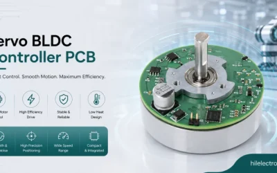
Servo and BLDC Controller PCB Design and Manufacturing
Servo and BLDC controller PCB guidance for FOC, encoder feedback, current sensing, EtherCAT, and calibration.
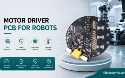
Motor Driver PCB for Robots: Power Stage, EMI and Protection
Motor driver PCB guidance for robot power stages, thermal design, current sensing, protection, and EMI control.
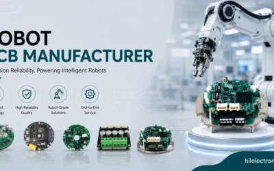
How to Choose a Robot PCB Manufacturer for Robotics Programs
A robot PCB manufacturer checklist covering fabrication, assembly, sourcing, test, documentation, and DFM support.