
Custom Backplane PCB Manufacturing by Highleap Electronic

Backplane PCBs are the backbone of high-speed and high-density electronic systems, enabling seamless communication and power distribution across multiple interconnected modules. Found in telecommunications, data centers, aerospace, and industrial applications, these specialized circuit boards are designed to handle complex interconnections and high-frequency signal integrity.
What Is a Backplane PCB?
A Backplane PCB is a highly specialized printed circuit board that serves as a central interconnection platform for multiple modules or daughter cards within a system chassis. It acts as the backbone of high-performance electronic systems, enabling high-speed communication and efficient power delivery across interconnected components. Unlike standard PCBs, Backplane PCBs are designed to handle advanced interconnect architectures, ultra-high-frequency signal transmission, and significant mechanical and thermal stresses, making them indispensable in industries such as telecommunications, data centers, aerospace, and industrial automation.
Key Characteristics of Backplane PCBs
1. High-Density Interconnects and Scalability
Backplane PCBs are engineered to accommodate high-density interconnections, supporting hundreds or even thousands of conductive traces and connectors. This is achieved through advanced technologies like differential pair routing for high-speed signaling, blind and buried vias for efficient space utilization, and press-fit or high-pin-count connectors to ensure robust mechanical and electrical performance. Their slot-based architecture provides modular scalability, allowing seamless integration of additional daughter cards or modules, making them ideal for systems requiring future-proof upgrades or reconfigurations.
2. Signal Integrity and Power Delivery
Maintaining signal integrity at multi-GHz frequencies is a cornerstone of Backplane PCB design. This involves controlled impedance transmission lines to minimize crosstalk and EMI, precise back-drilling techniques to eliminate via stubs, and high-quality laminates with ultra-low loss tangents for optimal high-speed signal propagation. For power delivery, Backplane PCBs use thick power and ground planes combined with strategically placed decoupling capacitors to ensure a stable power supply across diverse voltage rails, even in high-current systems, supporting demanding applications like data centers and telecommunications.
3. Thermal and Mechanical Robustness
Backplane PCBs are designed to withstand the challenges of high-power and high-density systems, incorporating advanced thermal management solutions such as thermally conductive materials, thermal vias, and optimized airflow pathways. Mechanically, they are reinforced with stiffeners and card guides to prevent flexing during frequent module insertions and removals, ensuring long-term reliability. Their ability to endure vibration, shock, and extreme temperatures makes them a critical choice for aerospace, defense, and industrial environments where operational reliability is paramount.

Devices That Require Backplane PCBs and Their Importance
1. Telecommunications and Data Centers
Backplane PCBs are integral to devices like 5G base stations, optical transport networks, servers, and network switches. These systems rely on Backplane PCBs to handle multi-Gbps data rates, ensure low-latency interconnections, and manage reliable power delivery across densely packed modules. In data centers, Backplane PCBs enable high-speed data transfer and modular scalability, supporting cloud computing and AI workloads. Their ability to maintain signal integrity and accommodate future upgrades makes them indispensable in telecommunications infrastructure and high-performance computing systems.
2. Aerospace, Industrial Automation, and Medical Devices
In aerospace and defense systems, such as avionics and radar, Backplane PCBs provide robust interconnections capable of withstanding extreme environmental conditions, including high vibration and temperature fluctuations. In industrial automation, they serve as the backbone for PLCs and robotic systems, ensuring real-time communication and scalability. Similarly, medical imaging devices like MRI and CT scanners depend on Backplane PCBs for high-speed data processing and precise power distribution, ensuring accurate and reliable diagnostics.
3. Automotive and Consumer Electronics
Modern vehicles, especially those with autonomous systems, rely on backplane PCBs for connecting radar, LiDAR, and communication modules within ADAS (Advanced Driver-Assistance Systems). Their durability ensures reliable operation in harsh automotive environments. In consumer electronics, Backplane PCBs simplify interconnections in high-end audio systems, modular gaming setups, and home automation hubs. Their ability to consolidate wiring, provide scalability, and ensure signal integrity supports efficient and streamlined designs, enhancing the user experience.
Backplane PCBs are at the core of advanced electronic systems across diverse industries, enabling seamless connectivity, high-speed data transfer, and reliable power distribution. From telecommunications and data centers to aerospace, industrial automation, automotive, and consumer electronics, these specialized PCBs provide the scalability, durability, and performance required in today’s most demanding applications. Their ability to handle complex interconnections and future-proof modular designs underscores their critical role in shaping the future of high-performance technology.
Backplane PCB Architecture
Designing a backplane PCB begins with careful interconnect planning, which involves defining the data rates, bandwidth requirements, and communication protocols to be supported. Protocols like PCIe, Ethernet, or proprietary buses are selected based on system performance needs. Detailed bandwidth analysis determines the number of lanes and channel capacities required for efficient data flow. Additionally, designers establish the interconnect topology, such as point-to-point or star configurations, to optimize communication between modules while maintaining signal integrity at high speeds.
Connector selection is another critical aspect of backplane PCB architecture. High-speed systems demand connectors capable of supporting data rates exceeding 25 Gbps, with robust mechanical designs to withstand frequent insertions and removals. High-density press-fit or elastomeric connectors are often chosen for their durability and space efficiency. Furthermore, impedance-matched connectors and shielding are essential to preserve signal quality and minimize electromagnetic interference (EMI), ensuring reliable performance in demanding environments like telecommunications or data centers.
The slot configuration and form factor define the physical layout of the backplane circuit board. Slots must be strategically spaced to accommodate daughter cards while ensuring adequate airflow for thermal management. Standardized form factors like ATCA, CompactPCI, or VMEbus are often used to ensure compatibility with existing chassis designs, while custom form factors are tailored for specialized applications. Proper alignment of slots and connectors minimizes signal trace lengths, reduces routing complexity, and ensures seamless integration with other system components. This architectural planning enables scalable, high-performance Backplane PCBs tailored to the needs of modern electronic systems.

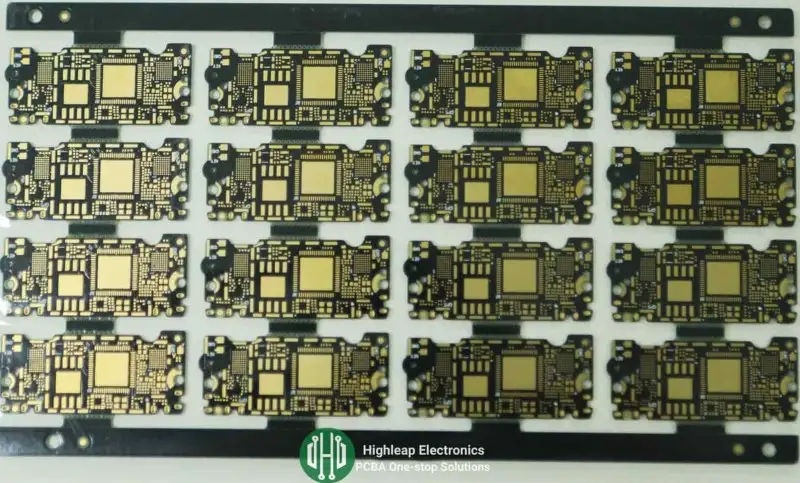
Backplane PCB Circuit Board
Considerations for Large-Format Backplane PCBs
In certain applications, the dimensions of backplane PCBs can far exceed those of standard PCBs, especially in high-performance systems like telecommunications switches, data center servers, and industrial automation platforms. Large-format Backplane PCBs are necessary to accommodate an increased number of slots, connectors, and interconnections. However, their design and manufacturing introduce unique challenges, requiring specialized techniques and materials to ensure optimal functionality and reliability.
1. Limitations in PCB Fabrication Equipment
Manufacturing large-format Backplane PCBs is constrained by the maximum panel size supported by standard PCB fabrication equipment, typically capped at dimensions such as 18×24 inches or 20×26 inches. Oversized boards often require custom fabrication processes, which involve panel stitching or step-and-repeat manufacturing to extend beyond conventional panel limits. These methods increase production complexity, lead times, and costs. Layer registration becomes particularly critical in large PCBs, as misalignments during lamination can lead to impedance mismatches, signal discontinuities, or via misregistration.
2. Mechanical Stability and Handling
Large backplane circuit boards are prone to flexural deformation, increasing the risk of microcracks in traces and vias. To ensure mechanical integrity, designers incorporate mechanical stiffeners, card retainers, and chassis brackets to minimize bending under operational stresses. Finite Element Analysis (FEA) is commonly used during the design phase to predict and mitigate warping or mechanical stress points. Additionally, handling oversized PCBs during fabrication and assembly requires precision equipment, such as vacuum tables and robotic handlers, to prevent damage from excessive flexure.
3. Signal Integrity Challenges
In large backplane PCBs, the extended trace lengths increase parasitic capacitance, inductance, and propagation delays, all of which degrade signal integrity. To address these challenges:
-
- Low-Loss Dielectric Materials: Advanced materials such as Rogers 4350B or Panasonic Megtron 6 are employed to reduce signal attenuation over long traces.
- Controlled Impedance Routing: Designers must ensure trace widths, spacing, and reference planes are tightly controlled to maintain consistent impedance for high-speed differential signals like PCIe Gen5 and 100G Ethernet.
- Via Optimization: Techniques such as back-drilling and stub elimination reduce signal reflections caused by unused via barrels, ensuring cleaner high-frequency performance.
- Advanced Simulation Tools: Signal integrity analysis using tools like HyperLynx or HFSS helps optimize trace layouts, differential pair skew, and return paths for high-speed designs.
4. Thermal Management in Large PCBs
Thermal dissipation is a critical factor in oversized backplane PCBs due to the high power density of connected modules. To address heat buildup:
-
- Thicker Copper Layers: Heavy copper planes (up to 4 oz) are used in power and ground layers to improve current carrying capacity and reduce resistive losses.
- Thermal Vias and Pads: Heat generated by power modules or high-speed ICs is dissipated through arrays of thermal vias that connect to heat sinks or thermally conductive layers.
- Active Cooling Solutions: Large Backplane PCBs are often integrated into systems with forced-air cooling, requiring optimized airflow pathways and provisions for active components like fans or liquid-cooled heat exchangers.
5. Manufacturing and Drilling Complexity
The high layer count and thickness of large backplane circuit boards, often exceeding 20 layers and 5 mm, create significant challenges in via drilling and plating. Key considerations include:
-
- Aspect Ratio Management: High aspect ratios (e.g., 10:1) in thick PCBs require precision drilling to ensure via reliability. Laser drilling or mechanical drilling with multiple passes may be necessary to achieve proper depth and alignment.
- Electroplating Uniformity: Ensuring even copper plating in high-aspect-ratio vias is critical for conductivity and mechanical robustness. Advanced plating techniques, such as pulse plating, are used to achieve uniform deposition.
- Stack-Up Design: The dielectric constant (Dk) and thickness of core materials must be carefully controlled to ensure consistency across all layers, particularly for controlled impedance designs.
Conclusion
Backplane PCBs serve as the critical foundation for high-speed, high-density electronic systems, seamlessly connecting multiple modules while ensuring reliable power distribution and uncompromised signal integrity. Their versatility and performance make them essential in driving advancements across industries such as telecommunications, data centers, aerospace, and automotive technology. With their ability to accommodate complex interconnections, support modular scalability, and withstand demanding environments, Backplane PCBs are pivotal in enabling next-generation electronic innovations.
At the forefront of backplane PCB manufacturing, Highleap Electronic offers cutting-edge solutions tailored to meet the specific needs of your systems. With expertise in large-format designs, high-speed signal integrity, and thermal management, we ensure your Backplane PCBs deliver superior performance and reliability. Partner with us today to unlock the full potential of your electronic systems and stay ahead in a rapidly evolving industry. Contact us to learn more about our customized PCB solutions!
FAQ for Backplane PCB
1. What materials are best suited for manufacturing high-speed Backplane PCBs?
For high-speed Backplane PCBs, materials like Rogers 4350B, Panasonic Megtron 6, and other ultra-low-loss laminates are ideal. These materials provide excellent signal integrity by minimizing dielectric loss and ensuring controlled impedance for GHz-level data transmission.
2. How can I ensure thermal management in densely packed Backplane PCB systems?
Thermal management can be optimized by using thicker copper layers for power planes, incorporating thermal vias, and ensuring adequate airflow through active cooling solutions like fans or liquid-cooled heat exchangers. Custom thermal designs tailored to your application ensure reliable operation in high-power systems.
3. What is the typical lead time for manufacturing complex Backplane PCBs?
The lead time for manufacturing a Backplane PCB depends on factors like layer count, board size, and custom requirements such as back-drilling or high-aspect-ratio vias. On average, production may take 1–2weeks, with expedited services available for critical projects.
4. Can Backplane PCBs be customized for specific form factors or unique applications?
Yes, Backplane PCBs can be fully customized to fit unique chassis designs or specialized applications. Customization may include specific dimensions, slot configurations, connector types, or material selections to ensure compatibility and optimal performance in your system.
5. What testing processes ensure the reliability of Backplane PCBs in high-performance environments?
Reliability testing for Backplane PCBs typically includes signal integrity simulations, power integrity analysis, thermal stress testing, and mechanical durability checks such as vibration and shock tests. These validations ensure the PCB performs consistently in demanding applications like aerospace, data centers, and telecommunications.
Get a Free PCB & PCBA Quote

Recommended Posts

PCB Manufacturing Process Flow – Ultimate Guide Is Here
[pac_divi_table_of_contents...

Exploring PCB Surface Treatment: The Significance of ENIG and DIG
PCB Surface Treatment:ENIG PCB With the ever-evolving...

How PCB Dry Film Plays a Key Role in Enhancing PCB Reliability
PCB dry film pressing equipmentWhat is PCB Dry Film? Dry...
High-Quality Rigid PCB Circuit Board Fabrication Services
HDI Rigid PCBWhat are rigid PCB and flexible PCB? In the...
How to get a quote for PCBs
Let us run DFM/DFA analysis for you and get back to you with a report.
You can upload your files securely through our website.
We require the following information in order to give you a quote:
-
- Gerber, ODB++, or .pcb, spec.
- BOM list if you require assembly
- Quantity
- Turn time
In addition to PCB manufacturing, we offer a comprehensive range of electronic services, including PCB design, PCBA (Printed Circuit Board Assembly), and turnkey solutions. Whether you need help with prototyping, design verification, component sourcing, or mass production, we provide end-to-end support to ensure your project’s success. For PCBA services, please provide your BOM (Bill of Materials) and any specific assembly instructions. We also offer DFM/DFA analysis to optimize your designs for manufacturability and assembly, ensuring a smooth production process.