
TMM10 PCB Manufacturing for Compact RF Designs

TMM10 PCB manufacturing is best suited to designs where high Dk is being used for compact RF geometry. The benefit is realized only when the finished stackup and small features remain consistent with the simulation. Rogers TMM10 is selected when RF size matters enough to justify a high dielectric constant. Rogers lists a process Dk of 9.20 ±0.230, a design Dk of 9.8 and a typical Df of 0.0022. Compared with a Dk near 3.5, the guided wavelength is shorter and many distributed structures can be reduced.
Miniaturization is not free. Lines and gaps become smaller, manufacturing variation consumes a larger percentage of the geometry, and parasitic effects from pads, vias, connectors and components become more important. A successful TMM10 project balances size reduction with build tolerance and testability.
Project review at a glance
| Best fit | Compact filters, resonators, couplers, matching networks, antennas, and modules where size reduction justifies higher geometry sensitivity. |
|---|---|
| Main manufacturing risk | Fine lines and gaps, pad/via parasitics, connector launches, and assembly tolerances consuming a larger share of the electrical design margin. |
| Expected engineering output | A manufacturable TMM10 construction with critical-dimension limits, assembly assumptions, prototype split options, and test correlation. |
The TMM10 manufacturing page focuses on compact RF production rather than repeating the fabrication sequence. The key inputs are miniaturized geometry, released stackup, production tolerances, first-article checks and the information needed for repeat orders.
How TMM10 Shrinks RF Structures
The electrical length of a transmission structure depends on effective dielectric constant. Increasing Dk shortens wavelength in the substrate, allowing resonators, matching lines, couplers and antenna elements to occupy less area. The exact reduction is topology-dependent; it should be calculated in an electromagnetic model rather than estimated from the Dk ratio alone.
TMM10 also offers TMM-family mechanical behavior, copper-matched CTE characteristics and thermoset processing. Rogers states that TMM10 and TMM10i can replace alumina substrates in some applications, giving designers another route to compact RF circuits with conventional PCB features.
For early trade-off work, see ways to reduce RF board area without losing manufacturability and how Highleap handles high-Dk Rogers laminates.
TMM10 vs RO4350B: Why Not Use the Lower-Cost Material?
| Decision factor | TMM10 | RO4350B | When it matters |
|---|---|---|---|
| Process Dk | 9.20 ±0.230 | 3.48 ±0.05 | TMM10 can substantially reduce distributed RF structures. |
| Design Dk | 9.8 | 3.66 | The two materials require different layouts and stackups. |
| Typical Df | 0.0022 | 0.0037 | TMM10 has the lower published dielectric-loss value. |
| Thermal coefficient of Dk | −38 ppm/°C | +50 ppm/°C | Temperature behavior differs in both magnitude and direction. |
| Flammability | Non-FR | UL94 V-0 | RO4350B may be preferable when V-0 is required. |
| Commercial route | High-Dk TMM material for compact circuits | FR4-like RF material for cost-sensitive multilayers | Use TMM10 only when miniaturization or approved performance offsets added material and tolerance cost. |
RO4350B is often the better answer when board area is available, V-0 is needed and conventional multilayer production cost is a priority. TMM10 becomes compelling when a resonator, antenna, matching network or module cannot meet the size target on a lower-Dk board.
When RO4350B is the alternative, compare its usual manufacturing route with the behavior of higher-Dk PCB materials before deciding that size reduction alone justifies TMM10.
TMM10 vs TMM10i: When Is Isotropic Dk Important?
TMM10i is identified by Rogers as an isotropic material with a process Dk of 9.80 ±0.245 and a design Dk of 9.9. TMM10 has a process Dk of 9.20 ±0.230 and a design Dk of 9.8. The “i” designation matters when the circuit model depends on dielectric behavior in multiple field orientations or when a previous qualification specifically requires the isotropic grade.
Do not substitute TMM10i for TMM10—or the reverse—because their names and design Dk values appear close. The specified grade, Dk model, thickness availability, program qualification and measured circuit correlation should control the decision. Highleap keeps the TMM10i material route separate for that reason.
High-Dk Build Conditions for TMM10
| Application | Benefit of high Dk | Trade-off to evaluate |
|---|---|---|
| Miniature resonators and filters | Shorter electrical length reduces circuit area. | Narrower absolute dimensions and tuning sensitivity. |
| Compact patch antennas | Smaller element size for a given frequency. | Potential efficiency and bandwidth trade-offs. |
| Power-amplifier matching networks | Short, compact distributed matching sections. | Current density, thermal path and component parasitics. |
| Oscillators and frequency-control circuits | Compact resonant structures with controlled substrate behavior. | Temperature correlation and shielding interaction. |
| Hybrid microwave modules | Can replace some ceramic-substrate functions while retaining PCB features. | Finish, wire bonding, die attach and mechanical flatness. |
The transition from a schematic value to copper geometry is covered in matching-network layout and impedance control.
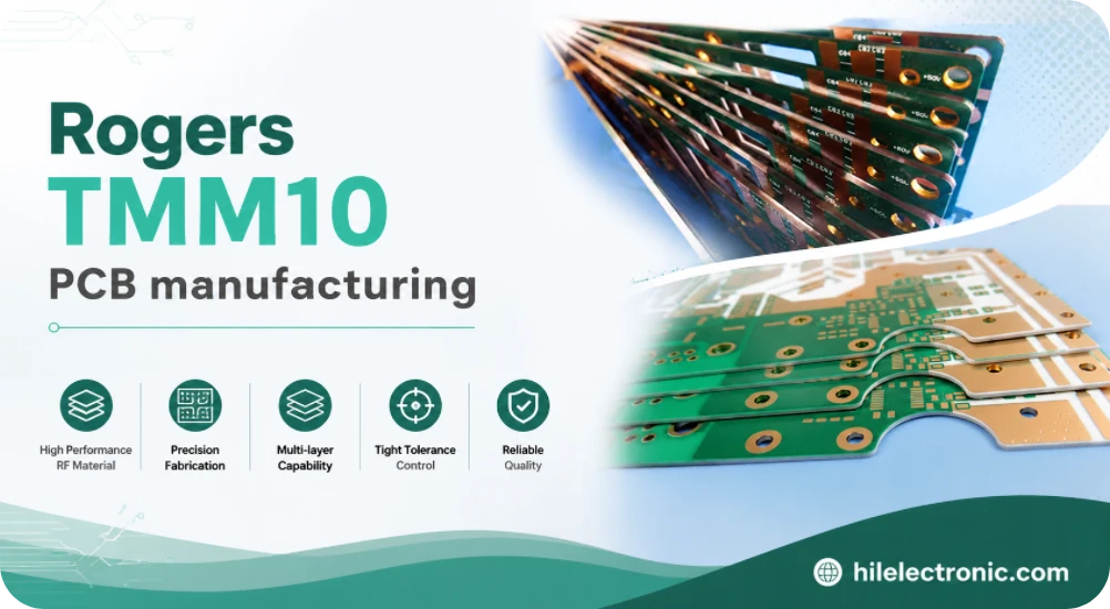
Material scope: This page concerns PCB fabrication using the specified Rogers material. Highleap Electronics manufactures the finished board and PCBA; laminate manufacturing and material sales are outside our service scope.
The Hidden Cost of RF Miniaturization
A smaller board is not automatically a cheaper board. TMM10 can reduce area but increase sensitivity to etched width, gap, registration, plating and component placement. Yield can decline if the design consumes the entire tolerance budget before fabrication begins.
- Fine coupling gaps may require tighter imaging and inspection.
- Small pads and short lines increase the effect of finish and solder fillets.
- Via inductance becomes a larger portion of the matching network.
- Connector launches can occupy more area than the RF circuit itself.
- Thermal density rises when power is concentrated into a smaller module.
- Manual tuning may become difficult if no access or trim feature is provided.
A practical design uses high Dk where it creates valuable size reduction and leaves adequate manufacturing margin everywhere else.
Layout and Assembly Choices for Compact TMM10 Modules
Compact modules benefit from a co-design review. Highleap checks the bare board together with the BOM, connector, shield, heat spreader and housing because these parts change parasitics and mechanical stress.
Wire-bonded or bare-die modules should define pad metallization, bond pull criteria and cleaning. Soldered modules should control paste volume, component stand-off and connector alignment. For finish selection, review pad and surface requirements for wire bonding and when ENEPIG supports mixed bonding and soldering.
When a Prototype Split Is Better Than One Frozen Design
For a sensitive first build, it can be more efficient to panelize two controlled geometry variants than to order one design and rely on manual rework. Examples include a small resonator-length split, two coupling-gap values, or two launch compensations. The variants must be intentional and documented; uncontrolled CAM changes are not an engineering experiment.
Highleap can review whether a split fits the same material panel and inspection plan. This approach is especially useful when simulation uncertainty is greater than the manufacturing tolerance and the result will be measured on a VNA.
TMM10 Material Decision Matrix
| Project condition | TMM10 decision |
|---|---|
| Board area is the dominant constraint and distributed RF structures are large. | Strong candidate; quantify the area saved against tolerance and cost. |
| UL94 V-0 is mandatory for the base laminate. | TMM10 is non-FR; evaluate an approved V-0 alternative or system-level compliance route. |
| The design already passes on RO4350B with available area. | Keep RO4350B unless TMM10 creates a measurable system benefit. |
| The circuit requires isotropic Dk correlation. | Compare TMM10i and confirm the specified material callout. |
| The module uses wire bonding or ceramic-style integration. | TMM10 may be attractive; review finish, flatness, die attach and thermal design. |
| The first build has no RF tuning or measurement plan. | Do not freeze production; define test and prototype learning first. |
Quote a Miniaturized TMM10 PCB or PCBA
Send the TMM10 or TMM10i grade, thickness, copper, Gerber/ODB++, drill, stackup, critical dimension table, EM model assumptions, surface finish, BOM, assembly drawing, housing data and RF acceptance plan. Identify the size target and which structures are permitted to change during DFM. Highleap checks the compact layers, vias, copper definition and assembly clearances before production. For miniaturized modules, the first article should validate both the PCB geometry and the component interface so the entire module remains aligned with the design intent. Exact material property values should be checked against the current supplier documentation for the specified grade and construction.
More detail on how TMM10 boards are fabricated is available for the production team. When the design is ready, send the files for a manufacturability and quotation review.
TMM10 DFM and Ordering Questions
How does TMM10 reduce RF circuit size?
Its higher dielectric constant shortens guided wavelength, which can reduce distributed structures. The actual reduction depends on topology, thickness, field distribution, copper, and the electromagnetic model.
Is TMM10 a drop-in replacement for RO4350B?
No. The dielectric constants differ substantially, so line widths, resonators, matching structures, launches, and the complete stackup must be redesigned and revalidated.
What is the main manufacturing risk with TMM10?
The same absolute etch or registration variation represents a larger percentage of narrow high-Dk geometry. Critical dimensions should be identified and measured.
When is a prototype split useful?
A split build can compare line compensation, finish, launch geometry, or tuning variants before one construction is frozen for production. For a TMM10 quote, include the modeled stackup, board size, critical dimensions, copper, finish, quantity and PCBA scope. This allows manufacturing and assembly to be planned as one build.
Related Rogers PCB Manufacturing Resources
- Rogers TMM PCB Manufacturer & Assembly Supplier
- Rogers TMM6 PCB for Microwave Filters
- Rogers TMM13i PCB Manufacturing & Feasibility Review
- Rogers TMM PCB Price, Cost Drivers & Quote Guide

Recommended Posts

TMM4 Filter PCB Manufacturing
TMM4 filter PCB manufacturing is controlled by the...

TMM3 PCB Manufacturing for RF Modules
TMM3 PCB manufacturing is most useful where the RF module...

TMM6 PCB Fabrication
TMM6 fabrication is the process-control page for a mid-Dk...
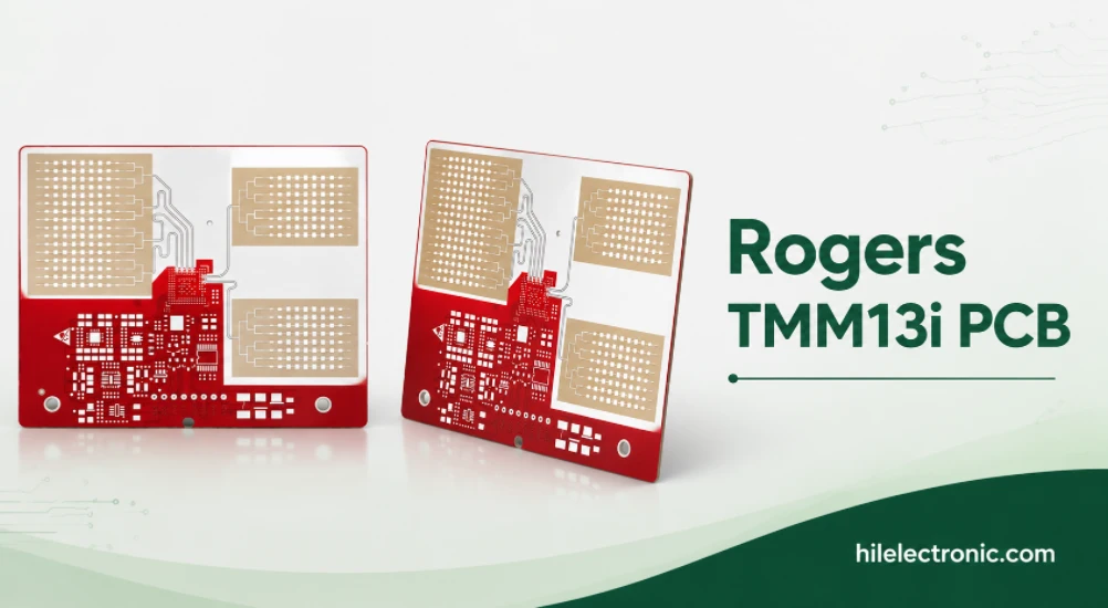
TMM13i PCB Manufacturing
TMM13i PCB manufacturing is aimed at ultra-compact RF...
How to get a quote for PCBs
Let’s run DFM/DFA analysis for you and get back to you with a report. You can upload your files securely through our website. We require the following information in order to give you a quote:
-
- Gerber, ODB++, or .pcb, spec.
- BOM list if you require assembly
- Quantity
- Turn time
For PCBA services, please provide your BOM (Bill of Materials) and any specific assembly instructions. We also offer DFM/DFA analysis to optimize your designs for manufacturability and assembly, ensuring a smooth production process.