
Best Rogers High-Dk PCB Materials for Compact RF Designs

As RF hardware becomes smaller and more integrated, engineers face a familiar problem: the enclosure keeps shrinking, but resonant structures such as patch antennas, couplers, filters, and matching sections still consume valuable board area. At that point, miniaturization can no longer rely on layout efficiency alone. The electrical behavior of the high-Dk PCB material becomes part of the design strategy itself.
That is where Rogers high Dk PCB fabrication becomes relevant. In many microwave and antenna designs, using a higher dielectric constant allows engineers to reduce circuit size while maintaining controlled RF behavior in compact RF PCB material and microwave PCB material applications. But selecting a high-Dk substrate is not simply a matter of choosing the highest number on a datasheet. Material family, processing method, thermomechanical stability, and fabrication tolerance all affect whether the finished board actually performs as intended.
This guide explains how high-Dk PCB material options from Rogers are used in compact RF and microwave designs, how to choose among common options such as Rogers RO3035, Rogers RO3006, Rogers RO3010, Rogers RO4360G2, and Rogers TMM10i, and what fabrication rules matter most when moving from simulation to production.
Request a Rogers High-Dk Fabrication Quote
Table of Contents
- What Is a High-Dk PCB Material and Why Does It Matter?
- What Are the Main Trade-Offs of High-Dk RF Design?
- How to Choose Between RO3035, RO3006, and RO3010
- When RO4360G2 Is a Better Manufacturing Choice
- Why TMM10i Is Used in More Demanding Environments
- Factory Execution: What Actually Determines Final RF Performance
What Is a High-Dk PCB Material and Why Does It Matter?
In RF and microwave design, a higher dielectric constant reduces the effective wavelength of the signal inside the substrate. That is why a high-Dk PCB material is often selected when the goal is to shrink the physical size of patch antennas, resonators, filters, couplers, and other distributed structures. In practical terms, the board material is no longer just a mechanical carrier. It becomes part of the electrical structure that determines impedance, phase response, coupling behavior, and resonant dimensions.
This is especially useful in systems where packaging constraints are severe, such as compact radar modules, dense wireless front ends, satellite communication hardware, and antenna networks that must fit inside limited mechanical envelopes. In those designs, reducing board size without losing predictable RF behavior can be more important than using the lowest-cost laminate. This makes material choice especially important in high frequency PCB material selection for compact antennas and microwave circuits.
However, high-Dk selection should always be tied to the real function of the circuit. Some projects need only modest miniaturization and stable microwave behavior. Others require aggressive size reduction in tightly constrained cavities. Still others care more about build consistency and manufacturing speed than maximizing dielectric constant. That is why a material selection decision should always consider both electrical goals and fabrication reality, not just a single Dk value.
What Are the Main Trade-Offs of High-Dk RF Design?
The main advantage of a high-Dk substrate is miniaturization. A higher dielectric constant allows RF structures to occupy less physical area, which helps designers free up routing space, shorten feed paths, and fit more function into a given enclosure. But this benefit comes with real trade-offs that must be managed early in the design phase.
The Miniaturization Benefit
For compact antennas, resonant structures, and tightly integrated microwave layouts, increasing Dk can produce meaningful footprint reduction without forcing a complete architecture change. This is one of the main reasons engineers compare materials such as RO3006, RO3010, and TMM10i when board space becomes limited. For teams evaluating how to choose high-Dk PCB material, the most important question is not the highest Dk value, but which material delivers the right balance of size reduction, electrical stability, and manufacturability.
The Manufacturing Cost of That Benefit
As dielectric constant increases, maintaining a target impedance often requires narrower trace geometry and tighter field control. That means the finished board becomes more sensitive to etch tolerance, copper profile, dielectric thickness, plated transitions, and stackup consistency. If the manufacturer cannot hold those build variables tightly enough, the electrical result may shift away from the simulated design.
In other words, high-Dk design is not just about choosing a better laminate. It is about accepting a narrower process window. The higher the electrical sensitivity of the circuit, the more important fabrication discipline becomes. This is also why the best high-Dk PCB material for RF design depends on the actual application rather than on dielectric constant alone.
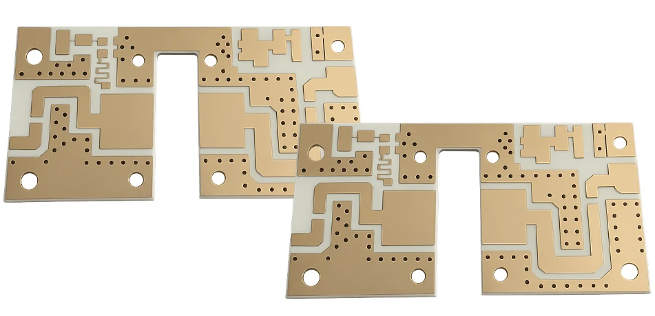
How to Choose Between RO3035, RO3006, and RO3010
Within the Rogers high-frequency material family, these three materials represent different levels of miniaturization and design intent. They should not be treated as interchangeable.
- Rogers RO3035: If the primary goal is stable dielectric behavior and predictable RF performance, but the design does not require extreme size reduction, Rogers RO3035 is a practical starting point. It fits RF signal paths, matching networks, couplers, filters, and antenna-related structures where material consistency matters and the design can tolerate a more moderate Dk.
- Rogers RO3006: When the layout needs more compact RF geometry while still prioritizing low loss and stable electrical behavior, Rogers RO3006 becomes a strong middle-ground option. It is commonly associated with filters, power amplifiers, couplers, antenna networks, and radar-related circuits where higher Dk helps reduce size without moving to the most aggressive miniaturization level.
- Rogers RO3010: For compact antenna layouts, resonant microwave structures, and other RF boards where the substrate is directly used to reduce circuit size, Rogers RO3010 is the more aggressive choice. It is suitable when space pressure is high, but it also places greater demands on trace accuracy, plated transition quality, stackup stability, and controlled assembly.
A simple way to think about the selection is this: RO3035 fits designs that prioritize stable RF behavior, RO3006 fits designs seeking a balance between size reduction and strong microwave performance, and RO3010 fits designs where compactness is a primary electrical requirement. For engineers comparing materials for high-Dk PCB material for antenna miniaturization, this progression provides a useful starting point.
It is also important not to force unrelated applications into the high-Dk category. For example, a fiber optic tether spool PCB may involve highly constrained geometry and demanding electromechanical integration, but its material priorities are driven by tension control, motor coordination, sensing, and system architecture rather than by high-Dk RF miniaturization alone. That makes it a useful example of space-constrained PCB design, but not proof that every unusual board shape requires a high-Dk substrate.

When RO4360G2 Is a Better Manufacturing Choice
One of the biggest practical issues in high-frequency manufacturing is that two materials can support similar design goals while behaving very differently on the factory floor. This is where Rogers RO4360G2 stands out.
RO4360G2 is positioned as a hydrocarbon ceramic-filled thermoset laminate with a dielectric constant of 6.15. That makes it especially attractive for teams that want meaningful RF miniaturization but also want a process flow closer to standard FR-4. Compared with PTFE-based approaches, this can simplify manufacturing and reduce some of the process bottlenecks associated with via preparation and hybrid production.
For many 5G front ends, broadband amplifiers, antenna subsystems, and mixed RF builds, the most useful material is not necessarily the one with the highest Dk. It is the one that balances electrical performance with scalable fabrication. In that context, RO4360G2 often becomes the more production-friendly answer, especially when lead time, repeatability, and manufacturability matter as much as RF compactness.
Why TMM10i Is Used in More Demanding Environments
When a design needs a dielectric constant near 10 but also requires strong dimensional predictability, Rogers TMM10i becomes highly relevant. It is described as a thermoset hydrocarbon resin heavily loaded with ceramic, providing an isotropic Dk of 9.80. That isotropic behavior is valuable in circuits where dielectric consistency in multiple axes contributes to more stable RF performance.
TMM10i is often considered for compact patch antennas, power amplifier boards, cavity-related structures, and microwave circuits where high Dk and stronger thermomechanical stability are both important. It can be a good fit for more demanding aerospace, satellite, and defense-oriented environments where designers want high electrical density without moving to brittle ceramic substrates.
That said, TMM10i should not be described as “immune” to reliability problems. A better way to frame it is that it can reduce risk in demanding environments when the design and build are both handled correctly. Its manufacturing challenge is different from PTFE-based materials: the dense ceramic loading can increase tool wear and make drilling and routing more difficult. So although it offers meaningful thermomechanical advantages, it still requires a supplier that understands the mechanical processing limits of the material.

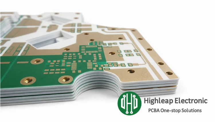
Factory Execution: What Actually Determines Final RF Performance
Choosing the right Dk value on paper does not guarantee a successful board. High-Dk RF performance depends on how well the design survives fabrication. That includes trace geometry control, copper definition, drilling quality, plating reliability, dielectric thickness consistency, lamination stability, and final assembly discipline.
As the substrate becomes electrically more influential, even relatively small geometric variation can matter more. Narrower traces, sidewall shape, copper weight, and plated transitions all contribute to the final impedance and tuned behavior of the circuit. That is why high-Dk builds usually require a more deliberate DFM review than standard RF boards.
For successful production, the factory should review at least the following items before release:
- Stackup accuracy: dielectric thickness and copper structure must support the intended impedance and field distribution.
- Trace definition: RF lines, resonant sections, and launch geometries need tighter dimensional control.
- Drilling and metallization: via quality, plating continuity, and material-specific preparation methods affect reliability and electrical repeatability.
- Copper weight selection: critical RF layers often benefit from thinner base copper to reduce profile distortion and keep geometry closer to design intent.
- Assembly control: connector alignment, ground continuity, stencil design, and thermal profile all influence final RF behavior.
That is why the broader value of Rogers high Dk PCB fabrication is not just material access. It is the ability to connect material choice, stackup planning, RF build strategy, and assembly execution into a repeatable production workflow.
Need help choosing the right high-Dk Rogers material?
Send your stackup, Gerber files, or RF design targets to our engineering team for a DFM review. We can help you compare RO3035, RO3006, RO3010, RO4360G2, and TMM10i based on miniaturization needs, fabrication complexity, and production readiness.

Recommended Posts
Rogers TMM6 PCB Manufacturing for Microwave Filters
Table of contentsWhy Microwave Filter Designers Use...
Taconic fastRise 27 Prepreg PCB Bonding and HDI Fabrication Service
Table of contentsWhat fastRise 27 Is—and What You Are...
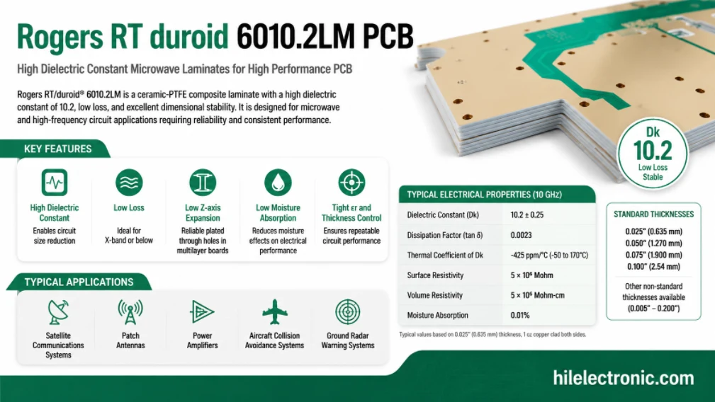
Rogers RT/duroid 6010.2LM PCB Manufacturer and Fabrication Service
Table of contentsIs RT/duroid 6010.2LM the Right Material...
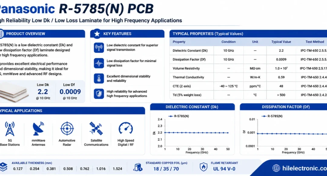
Panasonic R-5785(N) MEGTRON 7 PCB Manufacturer and Fabrication
Table of contentsWhen a Design Should Move to R-5785(N) /...
How to get a quote for PCBs
Let us run DFM/DFA analysis for you and get back to you with a report.
You can upload your files securely through our website.
We require the following information in order to give you a quote:
-
- Gerber, ODB++, or .pcb, spec.
- BOM list if you require assembly
- Quantity
- Turn time