
Tablet Computer PCB Manufacturing for Thin, Battery-Powered Devices
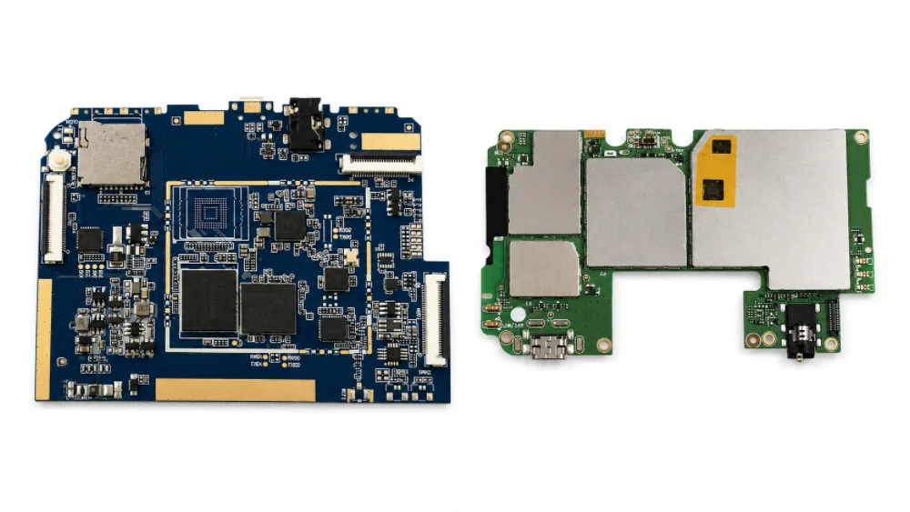
Table of contents
- Tablet Computer PCB Architecture in a Thin Mechanical Envelope
- Display, Touch and Flex Interconnect Manufacturing
- Battery Management, Charging and Power Distribution
- Wireless, Optional Cellular RF and Noise Control
- HDI, Fine-Pitch BGA and Thin Board Construction Where Applicable
- Thermal Management Without a Desktop-Class Cooling Envelope
- Tablet PCBA Assembly, Inspection and Interface Testing
- Sourcing and RFQ Requirements for Tablet Computer PCB Programs
A Tablet Computer PCB has to fit computing, display, touch, battery, wireless and sensor functions into a thin mechanical envelope. That combination creates different manufacturing priorities from a Chromebook or desktop motherboard even when both products use powerful application processors.
A tablet may use one mainboard plus flex cables, antenna modules or smaller interface boards, or it may consolidate more functions on a single rigid board. The correct manufacturing description must follow the released architecture rather than assume that all tablets use rigid-flex, HDI, cellular radios or multiple PCBs.
Highleap Electronics can support customer-owned tablet hardware from PCB fabrication through SMT/BGA assembly, sourcing, inspection and customer-defined testing.
1. Tablet Computer PCB Architecture in a Thin Mechanical Envelope
The mainboard commonly coordinates an application processor or SoC, memory, storage, display and touch interfaces, charging and power management, Wi-Fi/Bluetooth and product-specific sensors. Cameras, speakers, microphones and buttons may connect directly or through flex assemblies. Cellular circuitry is present only in designs that require it.
Tablet electronics are constrained by thickness before many other decisions are made. The mainboard must coexist with a large battery, display stack, cameras, speakers, antennas and structural parts, so component height, connector orientation and flex exit direction can be as important as board area. A production-ready design should identify keep-outs for the enclosure and battery, allowable board thickness, stiffener locations and any zones where mechanical pressure could be transferred into BGA or connector solder joints.
Architecture-to-manufacturing translation
| Design area | Manufacturing concern | Why it differs from a larger computer board |
|---|---|---|
| Processor / memory | Fine-pitch escape, power distribution, reflow | Less board area is available for fan-out and thermal spreading. |
| Display / touch | Connector placement, controlled routing, flex mating | The PCB must align with a large, thin display stack. |
| Battery / charging | Current paths, connector polarity, thermal density | The energy source is inside the same thin enclosure. |
| Wireless / optional cellular | Keep-outs, grounding, approved RF parts | Antenna and enclosure interactions are mechanically sensitive. |
| Cameras / sensors | Small connectors and orientation control | Many functions are distributed around the perimeter. |
Architecture also varies widely. Some tablets use a compact mainboard plus several flex circuits; others integrate more functions on one rigid or rigid-flex assembly. Manufacturing content should therefore describe the released partition rather than implying a universal multi-board architecture. During RFQ review, the supplier needs the mechanical drawings and flex mating information early enough to evaluate assembly sequence, panelization and test access instead of discovering those constraints after PCB tooling.
The thin enclosure changes how electrical and mechanical decisions interact. Processor, memory and storage placement compete with the battery volume, camera locations, speakers, antennas and the display stack. Even when the main PCB is rigid, multiple flex interconnects can bring cameras, buttons, touch sensors or daughter functions back to the board perimeter. That means connector datum, insertion direction and keep-out height are manufacturing parameters, not just industrial-design details.
For NPI, the board should be reviewed against the mechanical model or released drawing so that shield cans, tall components, FPC connectors and test points do not collide with the battery or enclosure. The same review should distinguish assembly options: a Wi-Fi-only SKU may share artwork with a cellular-capable platform but populate different RF or SIM-related components. A clear option matrix avoids purchasing parts or running tests that belong to another configuration.
- Mainboard outline and connector datum must match the display/battery mechanical stack.
- FPC/board-to-board connector orientation should be checked against assembly sequence and serviceability.
- SKU-specific RF, camera, storage or sensor options should be controlled by a population matrix.
- Test access should be designed before the enclosure removes physical access to important nodes.
2. Display, Touch and Flex Interconnect Manufacturing
The display and touch subsystem makes tablet PCB layout mechanically dependent. Connector position, mating direction, flex bend allowance and enclosure stack-up can be as important as the electrical netlist. An electrically correct mainboard can still fail integration if the display or touch flex cannot seat without stress.
Display and touch paths combine high pin density with mechanically sensitive interconnects. The host-to-display interface, touch-controller connection and panel flex arrangement may use different signaling standards depending on the product, but all rely on controlled connector geometry and clean routing. Fine-pitch FPC connectors are particularly sensitive to paste volume, coplanarity and post-reflow inspection because a small placement error can create an intermittent fault that appears only after repeated flex insertion.
Where the design uses flex or rigid-flex, the manufacturing package should define layer construction, stiffeners, coverlay, bend regions and connector geometry. Manufacturing review can address applicable flexible PCB or rigid-flex PCB requirements without assuming that these constructions are mandatory for every tablet.
Mechanical/electrical interface
Keep the PCB outline, connector datum, display stack and battery volume under one revision-control process. Late mechanical changes can invalidate routing clearance or flex geometry even when the schematic is unchanged.
Where a rigid-flex or separate flex interconnect is used, bend radius, copper grain direction, stiffener thickness and transition-zone design belong to the manufacturing package. The assembler also needs a handling method that prevents flex creasing during SMT and final integration. The commercial value of a supplier is therefore not simply ‘can make flex PCB’; it is whether the rigid, flex and assembly processes are coordinated around the actual fold geometry and final enclosure.
Display and touch links can be electrically fast, mechanically delicate or both. The manufacturing package should therefore define not only connector footprints but also mating flex drawings, stiffener thickness, contact orientation and insertion constraints. A few tenths of a millimeter of connector misalignment can create assembly stress even if the PCB outline itself is within tolerance. This is one reason board outline, slot and connector-datum measurements should be part of first-article mechanical inspection.
Noise control matters because touch-sensing circuits can coexist near display switching, high-speed digital lines and DC-DC converters. The product design determines filtering and grounding, but manufacturing must preserve the intended component values, reference paths and shielding features. If a touch-controller or display-bridge alternate is proposed during sourcing, it should be treated as an engineering change rather than a simple BOM substitution because firmware, timing, package escape and EMC performance may change.
Integration checkpoint
Before releasing the PCB, freeze the display and touch module part numbers—or explicitly define approved alternates—and include the mating flex data. This reduces the risk of a board that passes electrical test but cannot be assembled reliably into the display stack.
3. Battery Management, Charging and Power Distribution
Tablet power architecture must support the processor and display while managing charging, battery protection interfaces and low-power operating states defined by the product. The PCB manufacturing task is to preserve current paths, copper geometry, via arrays and component footprints that implement that power design.
Battery-powered tablets demand a disciplined power tree. Charging input, battery protection, fuel gauging, system rails and high-load processor/display domains must operate together, yet their detailed implementation varies by platform. The PCB should maintain short high-current loops, appropriate sense routing and separation between noisy switching nodes and sensitive analog/RF circuits. Component substitutions in charging or protection circuits should not be accepted solely because voltage and package appear similar.
USB-C may be used for charging and data, but the connector alone does not define Power Delivery or video support. Those functions depend on the port controllers, power path and system architecture. For this reason, production test should verify only the modes specified by the customer rather than assume a “full-featured USB-C” implementation.
High-current paths
Review neck-downs, via fields, connector pads and copper balance around charging and regulator circuits.
Battery interface
Control connector polarity, mechanical clearance and customer-defined protection/test requirements.
Power sequencing
Use firmware and acceptance criteria supplied for the released hardware revision.
From a manufacturing perspective, battery and charging connectors deserve mechanical as well as electrical review. Polarity, retention, mating height and nearby copper all influence integration risk. For NPI, define how the factory will verify charging detection, current-path continuity and relevant power rails without claiming to validate the complete battery pack or product safety certification. This creates a clear test boundary that procurement can quote and engineering can approve.
Battery-powered products need power-domain discipline because every unnecessary leakage path affects standby behavior and every high-current charging path affects heat. The PCB supplier should reproduce power-plane geometry, current-sharing vias, exposed-pad thermal vias and connector copper exactly as released. The assembler should also verify battery-connector polarity and package orientation for chargers, protection devices and regulators during first article because a repeated polarity or variant error can damage expensive assemblies.
Charging validation should be tied to the intended source and battery configuration. A Type-C receptacle may support simple USB charging or a negotiated USB Power Delivery implementation depending on the design. Test equipment, cables and firmware need to match that role. Where current limits or charge profiles are customer-defined, the production test should record measurable criteria—such as negotiation state, rail voltage, current range or temperature threshold—rather than a vague “charging works” result.
Manufacturing review for power sections
If the tablet uses a high-current charging path or tight battery clearance, Highleap can review copper neck-downs, via fields, connector pads, thermal reliefs and assembly clearances together with the released stack-up before the first lot.
Highleap Electronics • PCB Manufacturing & PCBA
Tablet PCB and PCBA Manufacturing Review
Send the mainboard, flex, power and test requirements for a controlled tablet build.
Request a Tablet PCB Quote →Discuss Tablet PCBA →
✓ DFM and DFA review ✓ Prototype to repeat production ✓ PCB fabrication and assembly
4. Wireless, Optional Cellular RF and Noise Control
Wi-Fi and Bluetooth are common tablet functions, while cellular connectivity is model-dependent. RF-enabled designs may add transceivers, front-end components, SIM/eSIM support and antenna connections, but these should never be implied on a Wi-Fi-only tablet.
Wi-Fi/Bluetooth and optional cellular functions are highly dependent on antenna placement, enclosure material and regulatory design. The PCB supplier should preserve RF keep-outs, reference-plane geometry, controlled RF feed structures and shielding footprints exactly as released. If modules are used, approved module variants and antenna connectors must be controlled; if radios are integrated directly, the RF component chain becomes even more sensitive to sourcing substitutions and assembly variation.
Manufacturing review should preserve RF keep-outs, grounding, shield-frame footprints and impedance-sensitive feed structures specified by the design team. Digital noise from the processor, memory and display should also be considered at placement and return-path boundaries.
Coexistence is also a layout and integration issue. High-speed display, memory and switching-power circuits can inject noise into radios or touch sensing, while cellular transmit activity can couple into audio or sensor paths. Factory DFM cannot replace RF validation, but it can flag unauthorized copper changes, shield-can conflicts, incorrect component populations and mechanical changes near the antenna region before those problems reach chamber testing.
Before tooling a thin tablet board
The most useful early review combines PCB data with the mechanical envelope, flex drawings, battery/display connectors and the fitted wireless options. That lets fabrication and assembly risks be closed before a thin-board or rigid-flex process is committed.
RF implementation is one of the strongest reasons not to treat all tablet motherboards as interchangeable. A Wi-Fi/Bluetooth design may use a module or discrete radio implementation, while a cellular SKU can add transceivers, front-end modules, filters, SIM/eSIM circuitry and multiple antenna connections. These additions change placement, shielding, power noise and test requirements. The manufacturing package should identify exactly which RF population belongs to each SKU.
For RF-sensitive zones, fabrication should preserve impedance-controlled feed geometry and copper keep-outs, while assembly should control shield-frame flatness, RF connector seating and approved matching components. Substitution risk is higher than it appears: a passive with the same nominal value can have different RF behavior, and an antenna cable or connector change can alter loss and mechanical fit. Production test may include basic communication checks, but final radiated performance and regulatory compliance remain system-level responsibilities unless a separate test scope is defined.
- Do not populate cellular front-end parts on Wi-Fi-only variants unless the released BOM requires them.
- Protect antenna keep-outs from late copper or mechanical changes.
- Treat RF matching networks and filters as controlled parts, not generic passives.
- Separate factory connectivity checks from final OTA/regulatory qualification.
5. HDI, Fine-Pitch BGA and Thin Board Construction Where Applicable
Thin products often drive component density, but density does not automatically mean a specific HDI stack-up. The need for microvias or sequential lamination depends on package pitch, escape strategy, board area and layer planning.
HDI is common in very space-constrained mobile electronics, but it should still be treated as a design choice rather than a category rule. When microvias, via-in-pad, fine lines or multiple sequential laminations are required, the supplier should review the exact buildup, aspect ratios, copper filling and registration strategy. The goal is to preserve escape density without creating a via structure that is unnecessarily difficult to manufacture or qualify.
If the released design requires HDI, Manufacturing review can address it through HDI PCB manufacturing. If conventional through-via multilayer construction meets the routing and thickness goals, it may be the more appropriate production route. The product category should not be used to overspecify the board.
Finished thickness, warpage risk, copper balance and registration are especially important when the PCB must fit against batteries, shields and display structures with limited z-height.
Thin boards introduce additional handling and flatness concerns. Panel support, tooling rails, copper balance and reflow fixtures may be needed to control bow and twist during assembly. Fine-pitch BGA and LGA packages amplify this issue because board deformation changes solder-joint collapse. A complete quotation should therefore include any special panelization, carrier or inspection steps required by the released thickness rather than treating a thin tablet PCB like a standard rigid board.
The manufacturing target is not “use HDI” but “reproduce the routing density with acceptable yield and reliability.” Fine-pitch BGAs can force smaller capture pads and tighter escape geometry; thin enclosures can limit finished board thickness; and component density can restrict test access. A DFM review should compare drill aspect ratio, laser-via structure, registration, annular ring and copper balance against the actual stack-up before tooling.
Sequential lamination also affects cost and lead time. Every build-up cycle adds process complexity, so stacked microvias should be used only where routing or via-in-pad geometry justifies them. If via filling and planarization are required under BGA pads, the fabrication note should say so explicitly. For thin boards, panel support and reflow warpage deserve attention because a PCB that is dimensionally acceptable at room temperature can still distort during assembly if copper distribution and thermal mass are highly asymmetric.
6. Thermal Management Without a Desktop-Class Cooling Envelope
A tablet enclosure provides limited volume for heat spreaders, graphite sheets or other product-level thermal hardware. PCB copper, thermal vias and component placement therefore participate in the heat path, but final temperature depends on the whole mechanical design and operating profile.
A tablet has little room for desktop-style heatsinks or fans, so thermal design usually relies on conduction and spreading through the board, shields, graphite, frames or other mechanical structures chosen by the product team. The PCB contribution is to preserve copper areas, thermal vias and component placement that support those paths. High-current regulators and charging devices should also be reviewed for local copper density so thermal relief decisions do not undermine current or heat flow.
Manufacturing review can address manufacturing implications using PCB thermal-management guidance, while the customer retains ownership of device-level thermal simulation and acceptance limits. This distinction prevents the factory from promising a final surface temperature that the bare board alone cannot guarantee.
Thermal risk is coupled to user comfort and battery aging, but the factory cannot validate those outcomes on a bare PCBA alone. NPI should define board-level checks—such as current consumption and temperature observation at agreed load points—separately from full-device thermal qualification. This gives buyers meaningful production evidence without turning the article into an unsupported claim that one PCB material or copper weight automatically solves tablet heat.
Tablet thermal design is dominated by the fact that heat has to leave a thin, mostly sealed enclosure without desktop-style airflow. The board may conduct heat into shields, graphite films, frames or other spreaders, but those interfaces are part of the product mechanical design. Manufacturing should preserve the contact locations, copper areas, exposed pads and via arrays that create the intended board-level path.
Assembly quality also affects thermal behavior. Insufficient solder under an exposed-pad power device, voiding outside the accepted process window or a lifted thermal interface can increase local temperature. Inspection and process development should therefore focus on the actual hot components identified by the design team. For validation, specify workload, ambient condition and measurement point; otherwise “thermal test” can produce inconsistent results across prototype and mass-production lots.
Useful conversion point
If your tablet PCBA has a known hot zone near the SoC, charger or display power circuit, provide the thermal-mechanical constraints with the Gerber/ODB++ package. Highleap can review manufacturability around thermal vias, copper balance and assembly access without claiming to replace system-level thermal qualification.
7. Tablet PCBA Assembly, Inspection and Interface Testing
Assembly typically involves small passives, fine-pitch ICs, board-to-board or FPC connectors and, in many designs, BGA packages. Stencil design, first-piece validation and stable reflow must account for mixed thermal mass and dense placement.
Tablet PCBA combines fine-pitch ICs with cameras, microphones, sensors, FPC connectors and shielding parts. First-piece verification is critical because orientation errors on repeated small connectors or sensors can be difficult to see after shields are installed. The process plan should define when shields are placed, which joints remain inspectable, and whether any connectors or modules need manual or secondary assembly after the main SMT reflow.
AOI is effective for visible placement and solder conditions; X-ray can be added for hidden joints where appropriate. Functional checks should then exercise the interfaces that actually exist on the SKU: display/touch communication, charging, USB, cameras, sensors, wireless and other customer-defined functions.
The manufacturing scope can combine SMT assembly with functional testing when fixtures, firmware and acceptance criteria are available.
Functional validation should be organized by interface: power and charging, display/touch, USB, wireless/module communication, cameras/sensors and audio where included. The factory should use customer-defined firmware, fixtures and acceptance limits; AOI or X-ray cannot substitute for these functional checks. For repeat builds, link the test profile to the exact SKU so optional cellular, memory or camera populations are not tested against the wrong configuration.
A thin tablet mainboard often combines fine-pitch components with fragile FPC connectors and mechanically exposed board edges. Stencil aperture design, board support, placement accuracy and reflow profile should account for this mix. Connector solder joints that look acceptable before enclosure assembly can fail later if the cable insertion direction or housing load was not considered, so first-article inspection should include mechanical mating where practical.
Functional test should follow the product architecture rather than a generic PCBA checklist. Display initialization, touch communication, camera buses, sensor interrupts, charging, USB, wireless and audio can each require different fixtures or software. It is usually more efficient to define a short manufacturing test that catches assembly faults and then leave full product validation to engineering. The key is traceability: record board revision, firmware, fixture version and test result so intermittent integration issues can be correlated to a specific build condition.
8. Sourcing and RFQ Requirements for Tablet Computer PCB Programs
A Tablet Computer PCB quotation should identify the hardware revision, fitted connectivity option, display/touch interface, battery connector, stack-up and any controlled-impedance requirements. Component substitutions need particular care where parts interact with firmware, RF performance, connector fit or power behavior.
Conclusion
Tablet PCB manufacturing is primarily a compact integration problem: thin mechanics, battery power, display/touch interconnects and optional RF functions have to be controlled together. The correct stack-up and assembly route should follow the released design rather than a generic “tablet board” template.
Tablet BOMs contain several parts that are poor candidates for uncontrolled substitution: processors, memory/storage, PMICs, display/touch controllers, cameras, RF devices, connectors and power components. Form and package equivalence does not guarantee firmware, timing, thermal or mechanical equivalence. Procurement should define approved manufacturers and alternates for these parts, while commodity passives can use a broader AVL when electrical requirements permit.
A strong RFQ makes the quotation comparable. Include the board stack-up, finished thickness, flex/rigid-flex details if used, controlled-impedance requirements, display/touch part numbers, battery interface, wireless variant, programming requirement and expected test coverage. Highleap can then separate fabrication, sourcing, assembly, inspection, fixture and test costs and identify which requirements drive lead time. That creates a clearer path from prototype to repeat production than quoting from Gerbers and a BOM alone.
RFQ conversion point
For a new Tablet Computer PCB build, send the released Gerber/ODB++, fabrication drawing, BOM, CPL, flex/mating drawings and test expectations together. The review can then focus on thin-board yield, connector mechanics, BGA process risk and variant control instead of generic tablet specifications.

Recommended Posts

TMM4 Filter PCB Manufacturing
TMM4 filter PCB manufacturing is controlled by the...

TMM3 PCB Manufacturing for RF Modules
TMM3 PCB manufacturing is most useful where the RF module...

TMM6 PCB Fabrication
TMM6 fabrication is the process-control page for a mid-Dk...

TMM10 PCB Manufacturing for Compact RF Designs
Table of contentsHow TMM10 Shrinks RF StructuresTMM10 vs...
How to get a quote for PCBs
Let’s run DFM/DFA analysis for you and get back to you with a report. You can upload your files securely through our website. We require the following information in order to give you a quote:
-
- Gerber, ODB++, or .pcb, spec.
- BOM list if you require assembly
- Quantity
- Turn time
For PCBA services, please provide your BOM (Bill of Materials) and any specific assembly instructions. We also offer DFM/DFA analysis to optimize your designs for manufacturability and assembly, ensuring a smooth production process.