
Comprehensive Guide to RF PCB Design

In the world of modern electronics, Radio Frequency (RF) Printed Circuit Boards (PCBs) are the foundation of a wide range of applications, from wireless communications and radar systems to satellite networks. Designing RF PCBs is a specialized process that requires expert knowledge, careful material selection, and precise layout techniques to achieve the desired performance. This comprehensive guide explores the critical considerations for RF PCB design, offering insights that will help you create high-performance boards while avoiding costly mistakes.
At Highleap Electronic, we specialize in delivering cutting-edge PCB manufacturing and assembly services tailored to your unique RF design needs. With decades of experience, we help you transform your designs into reliable products that perform flawlessly, no matter how demanding the application.
Understanding RF PCB Design Requirements
Before embarking on the design journey, it’s crucial to comprehensively understand the specific requirements of your RF PCB project. This foundational step ensures that all subsequent design decisions align with the intended application and performance goals.
Key Requirements to Assess:
- Operating Frequency Range: Determines the choice of materials and layout strategies.
- Input/Output Power Levels: Influences thermal management and component selection.
- Signal Types: Whether analog, digital, or a combination, each type has unique handling needs.
- Number of PCB Layers: Affects routing complexity and impedance control.
- Impedance Control Specifications: Critical for signal integrity, especially at high frequencies.
- Primary Routing Paths: Identifies main signal flows and potential interference zones.
- Shielding Requirements: Essential for minimizing electromagnetic interference (EMI).
- Thermal Design Constraints: Ensures effective heat dissipation to maintain component reliability.
- Technology Nodes for Active Components: Impacts the integration and performance of ICs.
- Compliance with Industry Standards: Ensures the PCB meets regulatory and performance benchmarks.
Selecting the Right Materials
The choice of materials profoundly impacts the RF PCB’s performance. Selecting substrates and conductors that align with your design’s frequency and performance requirements is paramount.
Material Considerations:
- Substrate Dielectric Constant: Materials like ceramics, PTFE, and low-loss laminates are favored for high-frequency applications due to their stable dielectric properties.
- Dielectric Tolerance: Tight tolerances minimize signal distortion and maintain impedance consistency.
- Copper Thickness and Plating: Ranging from 1 oz to 2 oz or thicker, the copper layer affects current handling and impedance.
- Conductor Finishes: High-performance finishes reduce signal loss and enhance durability.
- Foil Types: Options include standard, modified, and hyperbolic foils, each offering different impedance control characteristics.
- Layer Count and Routing Density: Adequate layers ensure sufficient routing channels without compromising signal integrity.
- Thermal Management: Thick cores can aid in heat sinking, essential for high-power applications.
Highleap Electronic offers a wide range of high-quality materials, ensuring your RF PCBs are built with the best substrates and conductors to meet your specific needs.

Mastering Impedance Control in RF PCB Design
Impedance control is the cornerstone of RF PCB design, ensuring high-speed signals propagate with minimal reflection and signal loss. For RF PCBs operating at multi-GHz frequencies, maintaining controlled impedance is critical to avoid performance degradation and data errors. Common impedance types include single-ended impedance, differential impedance, and coplanar waveguide impedance, each tailored to specific circuit requirements.
Steps to Achieve Controlled Impedance
- Determine Target Impedance: Typical values are 50Ω for most RF systems and 75Ω for broadcast applications, with differential impedance values calculated based on paired signal traces.
- Utilize Plane Layers: Ground or power planes are used as reference layers to stabilize impedance and reduce noise.
- Select Dielectric Thickness and Copper Weight: The dielectric constant, thickness, and copper weight directly affect impedance. Thinner dielectrics and lower copper roughness improve precision.
- Define Impedance in Fabrication Notes: Clear documentation prevents manufacturing errors and ensures that the PCB meets the design requirements.
- Leverage Simulation Tools: Tools like 3D electromagnetic solvers or advanced impedance calculators help accurately predict dimensions and optimize trace layouts.
- Specify Tolerances: Tight tolerances during fabrication maintain the integrity of single-ended, differential, or coplanar impedance.
Our Expertise in Impedance Control
At Highleap Electronic, we utilize cutting-edge techniques to maintain precise impedance levels across various configurations. Whether your design requires single-ended impedance for antenna feeds, differential impedance for high-speed data lines, or coplanar waveguide impedance for noise-sensitive circuits, our solutions ensure that RF signals remain pristine from design to production. Let us handle the complexities of impedance control, so you can focus on innovation.
Effective Isolation of Noisy Circuits
Minimizing electromagnetic interference is vital for maintaining signal clarity, especially in mixed-signal environments.
Isolation Strategies:
- Inner Layer Placement: Position noisy digital traces on inner layers, surrounded by ground planes to contain interference.
- Shielded Lines: Utilize shielded clock and data lines to prevent noise coupling.
- Metal Channels for Switching Supplies: Enclose switching-mode power supplies to contain noise within designated areas.
- Interface Shielding and Filtering: Protect sensitive interfaces with appropriate shielding or filtering mechanisms.
Expertise in isolation techniques ensures your RF PCB maintains high signal integrity even in challenging environments.
Ensuring Signal Integrity in RF PCB Design Through Isolation and Layer Optimization
Maintaining signal integrity in RF PCB design is essential, particularly in high-frequency and mixed-signal environments. Effective isolation techniques and strategic layer optimization play a critical role in minimizing electromagnetic interference (EMI) and preventing cross-talk, ensuring the clear and reliable transmission of signals.
Isolation Techniques for Noisy Circuits in RF PCB Design
- Inner Layer Placement: Position noisy digital traces on inner layers, surrounded by ground planes, to contain interference and shield sensitive analog or RF signals.
- Shielded Clock and Data Lines: Utilize shielded lines for critical clock and data signals to block noise coupling and improve overall signal stability.
- Metal Enclosures for Power Supplies: Enclose switching-mode power supplies in metal channels to reduce their noise and prevent interference with surrounding circuits.
- Interface Shielding and Filtering: Apply proper shielding or filtering mechanisms to protect sensitive interfaces, such as RF connectors, from external noise sources.
Layer Optimization Strategies for RF PCB Design
- Dedicated Ground and Power Planes: Implement solid ground and power planes to ensure low-impedance current flow, stabilize signals, and minimize noise.
- Interleaved Signal Layers: Position signal layers between ground planes to enhance isolation and reduce EMI and cross-talk, improving signal quality.
- Copper Flooding: Cover unused areas on inner layers with copper to act as a shield, maintain consistent impedance, and improve thermal management.
- Top and Bottom Layer Designation: Reserve the top layer for routing RF traces and the bottom layer for component placement to maximize space and ensure signal integrity.
At Highleap Electronic, we specialize in delivering advanced RF PCB design solutions that prioritize signal clarity and performance. By combining effective isolation techniques and innovative layer management strategies, we create RF PCBs tailored to meet the demands of high-frequency, high-speed, and mixed-signal environments. Contact us today to learn how we can help optimize your PCB design for maximum reliability and efficiency.
Optimizing RF PCB Design with Strategic Placement and Precision Routing
Achieving high performance in RF PCB design requires a combination of strategic component placement and precision routing techniques. By carefully managing signal paths and maintaining impedance continuity, you can minimize interference, reduce signal degradation, and enhance the overall efficiency of your PCB layout.
Strategic Component Placement in RF PCB Design
- Prioritize Active Components: Place ICs and active devices first, ensuring they are well-isolated from noisy areas for stable signal operation.
- Position Bypass Capacitors Close to ICs: Decoupling capacitors should be located as close as possible to power pins to stabilize voltage and minimize noise.
- Optimize Orientation for Routing Efficiency: Align components to allow for short and direct signal paths, reducing delays and improving signal integrity.
Efficient Routing Techniques for RF PCB Design
- Use 45° Angled Traces: Avoid 90° bends to reduce signal reflections and maintain impedance continuity, crucial for high-frequency applications.
- Route Critical Nets First: Ensure essential signals, like clocks and RF traces, are prioritized during the routing process to protect their integrity.
- Group Related Signals: Organize related signals into channels to minimize cross-talk and simplify the layout.
- Incorporate Smooth Curved Bends: Use curved and tapered bends to preserve impedance and avoid signal disruptions.
- Avoid Stubs and Acute Angles: Eliminate sharp bends and unnecessary vias that can cause reflections and degrade signal quality.
At Highleap Electronic, we specialize in RF PCB design, ensuring optimal placement and routing techniques for high-frequency applications. Whether you’re designing for wireless communication, radar systems, or IoT devices, our expertise will help you achieve reliable, high-performing RF PCBs. Contact us today to elevate your designs!
Advanced Modeling and Simulation Techniques for RF PCB Design
Leveraging advanced modeling and simulation tools is essential for predicting and optimizing RF PCB design performance before fabrication. These techniques minimize design errors, reduce costly re-spins, and ensure your product meets rigorous performance standards.
Key Simulation Techniques
- 3D Electromagnetic (EM) Simulation:
Tools like Ansys HFSS or CST Studio Suite provide detailed insights into signal behavior, identifying potential resonances, coupling issues, and electromagnetic interference. This ensures clean signal propagation and reliable operation. - Thermal Modeling:
Multiphysics solvers simulate airflow and heat transfer, helping to identify hotspots and implement effective thermal management strategies like heat sinks or thermal vias to improve reliability under high-power conditions. - Power Integrity Analysis:
Simulates power delivery networks to ensure stable voltage across the PCB. Identifies inrush current risks, potential voltage drops, and optimal decoupling capacitor placement for clean power distribution to RF components. - Signal Integrity Simulation:
Validates high-speed data links, minimizing noise coupling, signal reflections, and timing discrepancies. Essential for maintaining the integrity of differential pairs and clock signals in high-frequency designs. - Antenna Design Optimization:
Full-wave 3D EM solvers optimize antenna placement, size, and performance directly within the PCB layout. This is critical for RF PCBs used in wireless applications like IoT, 5G, and radar systems. - Manufacturing Variability Analysis:
Predicts the impact of fabrication process variations (e.g., dielectric thickness, copper roughness) on impedance and overall performance. This ensures design robustness and minimizes issues during production.
Why Advanced Simulation Matters
Advanced modeling tools not only improve signal clarity, thermal stability, and power distribution but also significantly reduce design cycles, saving time and costs. By identifying potential issues before fabrication, these techniques ensure your RF PCB performs reliably in high-frequency applications.
At Highleap Electronic, we leverage state-of-the-art simulation tools to ensure your RF PCB design is optimized for performance, reliability, and manufacturability. Contact us today to learn how our expertise can accelerate your product development while minimizing risks.
The RF PCB Design Workflow
A structured and iterative design workflow ensures that all aspects of RF PCB design are meticulously addressed, from initial concept to final production.
Step-by-Step Process:
- Schematic Design: Develop detailed circuit schematics incorporating all RF components, interconnects, and interfaces.
- Stackup Definition: Select appropriate dielectric materials, conductor weights, and layer counts based on design requirements.
- Component Placement: Strategically position active and passive components, considering signal flow and thermal management.
- Routing: Implement controlled impedance routing, maintain isolation between sections, and ensure efficient grounding.
- Modeling and Simulation: Conduct comprehensive simulations to validate EM, thermal, power, and signal integrity.
- Prototyping: Fabricate prototype boards for real-world testing and validation of design assumptions.
- Measurement and Tuning: Perform extensive testing to measure resonance, radiation, power consumption, and data rates, making necessary layout adjustments.
- Production Release: Finalize fabrication documentation and commence volume production once the design meets all performance criteria.
Highleap Electronic supports you through every stage of this workflow, providing expert guidance and high-quality manufacturing and assembly services to bring your RF PCB designs to life.
Mastering RF PCB Design with Highleap Electronic
Designing high-performance RF PCBs is a challenging but highly rewarding process that requires expertise in materials, precise layout strategies, and advanced simulation techniques. By implementing the best practices outlined in this guide, engineers can overcome the complexities of RF PCB design to ensure signal integrity, reduce losses, and achieve exceptional performance across diverse applications such as 5G, IoT, satellite communication, and radar systems.
Elevate your RF PCB designs with expert strategies that deliver superior results, enabling you to stay ahead in the rapidly evolving world of electronics.
Partner with Highleap Electronic—your trusted PCB manufacturing and assembly expert. With state-of-the-art technology, industry-leading quality, and customized solutions, we bring your innovative designs to life with unmatched precision and reliability. Contact us today to unlock the full potential of your RF PCB projects!
FAQ on RF PCB Design
What industries benefit most from RF PCB design?
RF PCB design is widely used in industries such as telecommunications (5G networks), aerospace (radar and satellite systems), automotive (advanced driver-assistance systems), IoT (smart devices), and medical (imaging and diagnostic equipment). These sectors rely on precise RF PCBs to enable high-frequency and low-loss signal performance.
How does RF PCB design impact wireless communication systems?
RF PCB design ensures efficient signal transmission and minimal interference, which are critical for wireless communication systems. Proper impedance control, shielding, and thermal management directly improve the performance of antennas, transmitters, and receivers in wireless networks.
What challenges can arise in RF PCB design during manufacturing?
Key challenges include maintaining consistent impedance during fabrication, achieving tight tolerances for high-frequency materials, and managing process variability such as dielectric thickness or copper roughness. Partnering with an experienced manufacturer ensures these issues are minimized.
Why is material selection so important in RF PCB design?
The choice of substrate material in RF PCB design affects dielectric constant, signal loss, and thermal management. Using low-loss materials like PTFE or ceramic-filled laminates improves high-frequency performance and ensures reliability in demanding applications.
How can Highleap Electronic help optimize RF PCB designs?
Highleap Electronic offers advanced manufacturing capabilities, expert design support, and precise assembly solutions to bring your RF PCB designs to life. With expertise in handling high-frequency layouts, material selection, and assembly integration, we ensure your RF PCB meets the highest standards of quality and performance. Contact us for customized RF PCB solutions.
Get a Free PCB & PCBA Quote

Recommended Posts
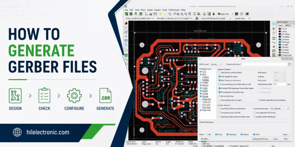
How to Generate Gerber Files for PCB Manufacturing
Figure 1. how to generate Gerber files image for Highleap...
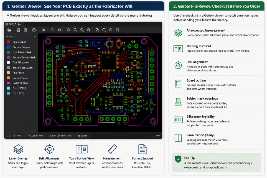
Gerber File Review Checklist: How to Check PCB Files Before You Order
Figure 1. Gerber file review catches missing layers, drill...
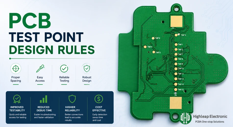
PCB Test Point Design Rules for Debug and ICT
Figure 1. PCB test point design rules help make debugging,...

PCB Jumper Wire: Uses, Types, and Design Tips
Figure 1. PCB jumper wires are useful for prototypes and...
How to get a quote for PCBs
Let us run DFM/DFA analysis for you and get back to you with a report.
You can upload your files securely through our website.
We require the following information in order to give you a quote:
-
- Gerber, ODB++, or .pcb, spec.
- BOM list if you require assembly
- Quantity
- Turn time
In addition to PCB manufacturing, we offer a comprehensive range of electronic services, including PCB design, PCBA (Printed Circuit Board Assembly), and turnkey solutions. Whether you need help with prototyping, design verification, component sourcing, or mass production, we provide end-to-end support to ensure your project’s success. For PCBA services, please provide your BOM (Bill of Materials) and any specific assembly instructions. We also offer DFM/DFA analysis to optimize your designs for manufacturability and assembly, ensuring a smooth production process.