
Essential PCB & PCBA Solutions for 5G Networks by Highleap Electronic

As the world rapidly transitions into the era of 5G networks, the demand for high-performance, reliable, and scalable infrastructure has never been greater. Central to the successful deployment and operation of these networks are sophisticated electronic components, particularly Printed Circuit Boards (PCBs) and their assembly (PCBA). These components form the backbone of the devices and systems that drive 5G technology, ensuring seamless connectivity, high-speed data transmission, and robust performance. In this article, we explore the critical equipment required to run 5G networks, delve into the specific PCB and PCBA requirements for these devices, and highlight how Highleap Electronic can be your trusted partner in designing and manufacturing top-tier PCB solutions.
Understanding the Core Equipment of 5G Networks
5G networks represent a significant leap from previous generations, offering enhanced speed, lower latency, and the ability to connect a vast number of devices simultaneously. To achieve these capabilities, a range of specialized equipment is essential. Below, we outline the key components and their associated PCB requirements.
1. 5G Base Stations
Macro Base Stations
Macro base stations are the primary nodes in a 5G network, providing broad coverage and handling high data throughput. These stations consist of several critical components:
-
-
Radio Units (RU): Responsible for transmitting and receiving radio signals, RUs require high-frequency PCBs capable of handling millimeter-wave (mmWave) frequencies. These PCBs must be designed with low-loss materials to minimize signal degradation.
-
Baseband Units (BBU): The brain of the base station, BBUs process incoming and outgoing data. They utilize multi-layer PCBs to accommodate complex digital and analog circuits, ensuring efficient data handling and processing.
-
Antenna Systems: Incorporating MIMO (Multiple Input Multiple Output) technology, antenna systems rely on high-precision PCBs to manage multiple signal paths and ensure optimal signal integrity.
-
Small Cells
Small cells complement macro base stations by providing localized coverage in high-density areas such as urban centers and stadiums. Due to their compact size, small cells utilize rigid-flex PCBs that offer both structural support and flexibility, allowing for intricate designs within limited spaces.
2. Core Network Equipment
The core network is the central hub that manages data traffic, routing, and overall network operations. Key components include:
-
-
Routers and Switches: These devices manage data flow within the network, requiring high-speed, multi-layer PCBs to handle large volumes of data with minimal latency.
-
Servers: Serving as the data processing and storage units, servers demand high-density PCBs with robust thermal management solutions to maintain performance under continuous load.
-
3. Fiber Optic Transmission Equipment
Fiber optic systems are integral to 5G networks, enabling high-speed data transmission between base stations and the core network.
-
-
Fiber Optic Transceivers: These components convert electrical signals to optical signals and vice versa. They require precision-engineered PCBs with excellent signal integrity to ensure reliable data transmission.
-
Optical Distribution Hubs: Managing and distributing optical fibers, these hubs use high-reliability PCBs designed for scalability and ease of maintenance.
-
4. Power Systems
Reliable power supply is crucial for maintaining network uptime and performance.
-
-
Uninterruptible Power Supplies (UPS): UPS systems ensure continuous power during outages, relying on efficient power management PCBs to regulate and distribute electrical power seamlessly.
-
Power Distribution Units (PDUs): PDUs distribute power to various network components, necessitating robust PCBs capable of handling high power loads and ensuring stable operation.
-
5. Cooling Systems
Effective cooling is essential to prevent overheating and maintain the longevity of network equipment.
-
-
Heat Sinks and Cooling Fans: These components use thermally conductive PCBs to dissipate heat efficiently, maintaining optimal operating temperatures for sensitive electronics.
-
Liquid Cooling Systems: For high-density setups, liquid cooling provides superior heat management. The PCBs in these systems must be designed with corrosion-resistant materials and high thermal conductivity to handle liquid-based cooling effectively.
-
6. Monitoring and Management Equipment
Continuous monitoring and management are vital for maintaining network performance and reliability.
-
-
Network Monitoring Tools: These tools utilize high-precision PCBs to collect and analyze real-time data, ensuring proactive maintenance and rapid issue resolution.
-
Remote Management Modules: Enabling remote control and configuration of network equipment, these modules require secure and reliable PCBs to safeguard against unauthorized access and ensure uninterrupted operations.
-

PCB & PCBA: The Heart of 5G Network Equipment
The performance and reliability of 5G network equipment heavily depend on the quality of their PCBs and the precision of their assembly. Here’s how PCBs and PCBA play a pivotal role:
High-Frequency PCBs
Operating at higher frequencies, 5G devices require PCBs made from materials with low dielectric loss and high thermal stability. Materials such as Rogers or Teflon-based laminates are commonly used to ensure minimal signal loss and excellent performance.
Multi-Layer and High-Density Interconnect (HDI) PCBs
To accommodate the complex circuitry and high component density of 5G devices, multi-layer and HDI PCBs are essential. These PCBs allow for intricate routing of high-speed signals, reducing electromagnetic interference (EMI) and ensuring signal integrity.
Rigid-Flex PCBs
Combining the rigidity of traditional PCBs with the flexibility needed for compact and dynamic applications, rigid-flex PCBs are ideal for small cell equipment and other space-constrained devices.
Advanced PCBA Techniques
The assembly of PCBs for 5G equipment involves sophisticated techniques such as:
-
- Surface Mount Technology (SMT): Ensures precise placement of high-density components essential for high-frequency applications.
- Ball Grid Array (BGA) Packaging: Provides reliable connections for complex ICs, critical for maintaining performance in demanding environments.
- Controlled Impedance Routing: Maintains signal integrity by ensuring consistent impedance throughout high-speed signal paths.
Testing and Quality Assurance
Rigorous testing processes, including automated optical inspection (AOI), in-circuit testing (ICT), and functional testing, ensure that each PCB and PCBA meets the stringent quality standards required for 5G networks.
Enclosure Design
Protective enclosures for 5G equipment must offer robust shielding against EMI, effective thermal management, and durability against environmental factors. High-quality enclosures are designed with materials like aluminum or high-grade plastics and incorporate advanced thermal solutions to maintain optimal operating conditions.
Why Choose Highleap Electronic for Your 5G PCB Needs
At Highleap Electronic, we understand the critical role that PCBs and PCBA play in the success of 5G networks. Our comprehensive capabilities include:
Custom PCB Design and Manufacturing
Whether you need high-frequency, multi-layer, HDI, or rigid-flex PCBs, our expert design team collaborates with you to create tailored solutions that meet your specific requirements. We utilize state-of-the-art manufacturing processes to ensure precision and reliability in every PCB we produce.
Advanced PCB Assembly Services
Our PCBA services encompass the entire assembly process, from component placement using advanced SMT and BGA techniques to thorough testing and quality assurance. We ensure that your PCBs are assembled to the highest standards, ready to perform flawlessly in demanding 5G applications.
Comprehensive Testing and Quality Control
Quality is at the forefront of everything we do. Our rigorous testing protocols, including AOI, ICT, and functional testing, guarantee that each PCB and PCBA meets the stringent performance and reliability standards required for 5G networks.
Expert Enclosure Design and Manufacturing
In addition to PCB and PCBA services, we offer custom enclosure design and manufacturing. Our enclosures are crafted to provide robust protection, effective thermal management, and EMI shielding, ensuring your 5G equipment operates smoothly in any environment.
End-to-End Solutions
From initial design and prototyping to full-scale production and assembly, Highleap Electronic provides end-to-end solutions tailored to your unique needs. Our experienced team works closely with you to ensure seamless integration and optimal performance of your 5G network equipment.
Why Choose Highleap Electronic?
-
- Cutting-Edge Technology: We leverage the latest advancements in PCB manufacturing and assembly to deliver high-performance solutions.
- Quality Assurance: Our commitment to quality ensures that every PCB and PCBA we produce meets the highest industry standards.
- Flexible and Scalable Production: Whether you’re a startup or a large enterprise, our scalable production capabilities can accommodate projects of any size.
- Experienced Team: Our skilled engineers and technicians bring extensive expertise to every project, ensuring successful outcomes.
- Customer-Centric Approach: We prioritize your needs, offering personalized support and solutions to help you achieve your goals.

Certifications and Qualifications
At Highleap Electronic, we are committed to delivering high-quality, reliable, and environmentally compliant PCB and PCBA solutions. Our certifications reflect our dedication to meeting global industry standards across various sectors, including telecommunications, automotive, aerospace, and medical devices. Key certifications include ISO 9001 for quality management, ISO 14001 for environmental management, IATF 16949 for automotive production, ISO 13485 for medical device manufacturing, and AS9100 for aerospace applications.
We also ensure compliance with crucial safety and environmental standards, such as RoHS and REACH, guaranteeing our products are free from hazardous substances and meet strict environmental requirements. Additionally, our UL-certified PCBs comply with stringent safety standards, while adherence to IPC-A-610 and IPC-6012 ensures precision and quality in PCB design, assembly, and inspection.
The certifications listed on our Certifications Page represent only a portion of the qualifications we hold. If you need more information or require details on specific certifications tailored to your project, please contact us directly. Our team will gladly provide the comprehensive documentation you need.
Contact Highleap Electronic Today
Ready to elevate your 5G network with high-quality PCB and PCBA solutions? Highleap Electronic is your dedicated partner in navigating the complexities of PCB design, manufacturing, and assembly for 5G network equipment. Our expertise and commitment to excellence ensure that your 5G projects are supported by the best possible electronic solutions.
Get in Touch with Us
- Phone: +86 13503062089, +86 13500039316, +86 18903006645, +86 18928950984
- Email: [email protected], [email protected], [email protected], [email protected]
- Inquiry Form: Complete our inquiry form to upload your files and get a free, fast quote.
We understand that many of our successful projects are bound by confidentiality agreements. While we cannot disclose specific case studies, we invite you to reach out to us directly to discuss how our solutions can meet your unique 5G requirements. Our team is ready to provide you with detailed information about our capabilities, certifications, and how we can support your next 5G project.
Conclusion
The deployment and operation of 5G networks require a complex ecosystem of advanced telecom and communication equipment, all of which are built upon the foundation of high-quality PCBs and precision PCBA. From base stations and core network devices to fiber optic transmission systems and cooling solutions, every component must meet the highest standards of performance and reliability to deliver the seamless connectivity and low latency that define modern telecommunication technology.
At Highleap Electronic, we specialize in meeting these exacting demands with cutting-edge PCB design, manufacturing, and assembly tailored for telecommunications and wireless communication applications. Our team brings unmatched expertise, state-of-the-art facilities, and a commitment to excellence to every project, ensuring that your 5G equipment is not only functional but optimized for peak performance and long-term reliability.
Partner with Highleap Electronic to Elevate Your 5G Telecom Infrastructure
With our comprehensive capabilities, including advanced PCB manufacturing, assembly, and testing, we are ready to empower your 5G projects with innovative and dependable solutions. Whether you are developing critical telecom infrastructure or next-generation communication devices, our expertise ensures seamless integration and superior results.
Contact Highleap Electronic today to discover how our capabilities can drive the success of your telecommunication and communication network projects and take your connectivity to the next level. Let us help you shape the future of communication with unparalleled precision, reliability, and innovation.
FAQs About 5G PCB & PCBA Solutions
1. What is the typical lead time for custom PCB manufacturing and assembly for 5G equipment?
For custom high-frequency or multi-layer PCBs designed for 5G applications, production and assembly typically take 5–10 days. Highleap Electronic also offers expedited services for urgent requirements and supports both prototype and full-scale production.
2. Can Highleap Electronic handle large-scale PCB production and assembly for 5G projects?
Yes, we excel in both small-batch and high-volume production. Whether you need a few prototypes for testing or mass production for large-scale deployment, we have the capacity and expertise to meet your needs efficiently.
3. How does PCB design influence the performance of 5G network devices?
PCB design plays a critical role in maintaining signal integrity, ensuring proper thermal management, and reducing electromagnetic interference (EMI). A well-optimized design directly impacts the efficiency and reliability of 5G network devices.
4. Does Highleap Electronic provide design assistance for 5G-specific PCB layouts?
Absolutely. Our engineering team offers comprehensive design support, helping clients optimize PCB layouts for high-frequency materials, controlled impedance, and advanced assembly requirements. This ensures your design is perfectly suited for 5G applications.
5. What materials are recommended for PCBs in 5G networks, and can Highleap source them?
Materials like Rogers, Taconic, and Teflon-based laminates are preferred for their low dielectric loss and high thermal stability. Highleap Electronic has a robust supply chain and can source these premium materials to meet the exact specifications of your 5G project.
Get a Free PCB & PCBA Quote

Recommended Posts
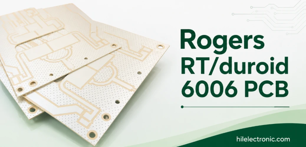
RT/duroid 6006 PCB Manufacturer for Compact High-Dk Microwave Circuits
RT/duroid 6006 is selected when circuit area is expensive....
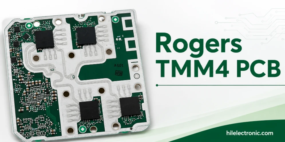
Rogers TMM4 PCB Manufacturer for Compact Microwave Filters
TMM4 is most useful when a microwave circuit must become...
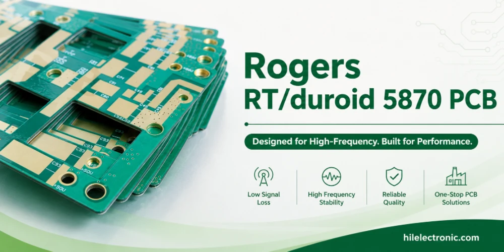
RT/duroid 5870 PCB Manufacturer for Low-Loss PTFE RF Circuits
RT/duroid 5870 is chosen when the RF path needs low loss,...
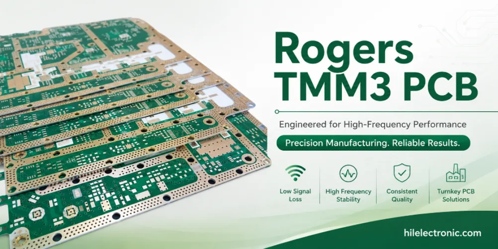
Rogers TMM3 PCB Manufacturer for Mechanical RF Modules
TMM3 is selected when an RF circuit must behave as part of...
How to get a quote for PCBs
Let us run DFM/DFA analysis for you and get back to you with a report.
You can upload your files securely through our website.
We require the following information in order to give you a quote:
-
- Gerber, ODB++, or .pcb, spec.
- BOM list if you require assembly
- Quantity
- Turn time
In addition to PCB manufacturing, we offer a comprehensive range of electronic services, including PCB design, PCBA (Printed Circuit Board Assembly), and turnkey solutions. Whether you need help with prototyping, design verification, component sourcing, or mass production, we provide end-to-end support to ensure your project’s success. For PCBA services, please provide your BOM (Bill of Materials) and any specific assembly instructions. We also offer DFM/DFA analysis to optimize your designs for manufacturability and assembly, ensuring a smooth production process.