
Comprehensive Guide to Semiconductor PCBs: Enhancing Modern Electronics

In the rapidly advancing world of electronics, Semiconductor PCBs (Printed Circuit Boards) stand as the foundational elements that drive innovation and functionality across a multitude of industries. Whether you’re developing cutting-edge consumer gadgets, sophisticated automotive systems, or critical healthcare devices, understanding Semiconductor PCBs is essential. At Highleap Electronic, a premier PCB manufacturing and assembly provider, we specialize in delivering high-quality Semiconductor PCBs tailored to meet your unique project requirements.
What is a Semiconductor PCB?
A Semiconductor PCB is a specialized printed circuit board designed to host and interconnect semiconductor devices such as integrated circuits (ICs), transistors, and diodes. These PCBs serve as the mechanical and electrical backbone for semiconductor components, enabling them to function cohesively within electronic systems.
Understanding Semiconductors
Semiconductors are materials that exhibit properties between conductors and insulators. They can conduct electricity under certain conditions, making them ideal for controlling electrical currents in devices. Common semiconductor materials include:
-
- Silicon (Si): The most widely used semiconductor material due to its abundance and excellent electrical properties.
- Germanium (Ge): Known for its high thermal conductivity, often alloyed with silicon for enhanced performance.
- Gallium Arsenide (GaAs): Utilized in high-speed and high-frequency applications, albeit more expensive than silicon.
Role of Semiconductor PCBs
While semiconductors handle the processing and control of electrical signals, Semiconductor PCBs provide the necessary support and connectivity. They ensure that semiconductor devices are securely mounted, properly interconnected, and effectively managed in terms of thermal dissipation and signal integrity.

Semiconductor PCB Design & Fabrication
Designing and fabricating a Semiconductor PCB is a meticulous process that requires precision and expertise. Here’s an overview of the key stages involved:
1. Design and Layout
-
- CAD Software: Utilization of Computer-Aided Design (CAD) tools to create detailed PCB layouts, ensuring accurate component placement and trace routing.
- Design for Manufacturability (DFM): Incorporating design principles that facilitate easier manufacturing and assembly, reducing potential errors and production delays.
- High-Density Interconnects (HDI): Implementing fine traces and microvias to accommodate complex circuitry in compact spaces.
2. Material Selection
-
- Substrates: Choosing appropriate dielectric materials such as FR4 for general-purpose PCBs or Polyimide for high-frequency applications.
- Copper Cladding: Selecting the right copper thickness to handle current loads and signal integrity requirements.
3. Layer Formation
-
- Multilayer Stacking: Laminating multiple layers of copper-clad substrates with insulating layers to build the core structure of the PCB.
- Prepreg Application: Applying pre-impregnated bonding sheets between layers to ensure strong adhesion during lamination.
4. Imaging and Etching
-
- Photolithography: Transferring the PCB design onto the copper layers using photoresist materials and UV exposure.
- Etching: Removing excess copper to create the desired trace patterns, ensuring precise electrical pathways.
5. Drilling and Plating
-
- Precision Drilling: Creating vias and through-holes using mechanical drills or laser systems for accurate placement.
- Electroplating: Depositing copper in drilled holes to establish electrical connections between different PCB layers.
6. Solder Mask Application
-
- Protective Coating: Applying a solder mask layer to shield copper traces from oxidation and prevent solder bridging during component placement.
- Customization: Utilizing various solder mask colors for aesthetic purposes and to differentiate between different PCB layers.
7. Surface Finishing
-
- Surface Treatments: Applying finishes like ENIG (Electroless Nickel Immersion Gold) or HASL (Hot Air Solder Leveling) to enhance solderability and protect exposed copper pads.
- Quality Control: Ensuring uniformity and adherence of surface finishes to maintain consistent performance.
8. Silkscreen Printing
-
- Legend Marking: Printing component outlines, reference designators, and other essential markings to guide assembly and troubleshooting processes.
- Customization: Incorporating logos or specific instructions as per client requirements.
9. Quality Assurance and Testing
-
- Automated Optical Inspection (AOI): Scanning PCBs for visual defects such as missing components or trace irregularities.
- Electrical Testing: Conducting tests like flying probe or in-circuit testing to verify electrical integrity and functionality.
- Environmental Testing: Assessing PCB performance under various conditions to ensure reliability.
Semiconductor PCB Assembly
The assembly process for Semiconductor PCBs is a critical stage in turning a manufactured PCB into a fully functional electronic system. At Highleap Electronic, we specialize in advanced PCB assembly methods to ensure reliability and efficiency, tailored to the needs of high-performance semiconductor-based designs.
Component Sourcing and Preparation: The process begins with sourcing high-quality components such as diodes, transistors, ICs, and passive elements. Each component undergoes rigorous verification to ensure it meets design specifications. Once validated, these components are prepared for automated assembly.
Mounting Technologies:
-
- Surface Mount Technology (SMT) is commonly used for compact and high-density designs. Components are placed directly onto the PCB surface using automated pick-and-place machines, offering precision and speed.
- Through-Hole Technology (THT) is employed for robust connections, especially for larger components that require enhanced mechanical strength.
- Mixed Technology combines SMT and THT for designs requiring a balance between high density and strong physical connections.
Assembly Workflow: The process includes solder paste stenciling, automated placement of components, reflow soldering for SMT parts, and wave soldering for THT components. Each step is carefully monitored to ensure accuracy and consistency.

Comprehensive Semiconductor PCB Testing
Testing is a vital phase in the production of Semiconductor PCBs, ensuring that every board meets stringent quality, performance, and reliability standards. At Highleap Electronic, we prioritize testing as an integral part of the manufacturing process, combining cutting-edge technology with meticulous methodologies to identify defects, verify functionality, and ensure long-term durability. This approach minimizes risks and guarantees that our PCBs are ready to perform in demanding applications across industries such as consumer electronics, automotive, and aerospace.
The testing process encompasses multiple methodologies tailored to uncover defects and verify every aspect of the PCB’s performance. Automated Optical Inspection(AOI) is conducted early in the process to detect surface-level issues like soldering defects, misaligned components, or missing parts. In-Circuit Testing(ICT) focuses on verifying the electrical properties of individual components, ensuring proper soldering, continuity, and resistance. For high-complexity designs, X-Ray Inspection is used to examine internal features such as buried vias and multilayer structures for hidden defects. Environmental Testing, including thermal cycling, vibration tests, and humidity exposure, is performed to simulate real-world conditions and assess the board’s durability. Finally, Functional Testing evaluates the fully assembled board under operational conditions, verifying power distribution, signal flow, and data communication to ensure the PCB performs according to design specifications.
At Highleap Electronic, our comprehensive testing framework ensures that every Semiconductor PCB we deliver is reliable, robust, and ready for deployment. By combining advanced testing technologies with our expertise in PCB manufacturing and assembly, we provide our clients with the confidence that their products will meet the highest standards of performance, even in the most demanding environments. Testing is not just a step in the process—it’s a commitment to quality and excellence.
Semiconductor PCB Enclosure
The enclosure is a vital aspect of the final product, protecting the Semiconductor PCB and ensuring its longevity and functionality in real-world applications. Highleap Electronic offers customized enclosure solutions tailored to the specific needs of your project.
Design and Material Selection: Enclosure design begins with selecting the right material. Options include plastics for lightweight and cost-effective solutions, aluminum for superior heat dissipation, and stainless steel for maximum durability. The design is optimized for functionality, including space for connectors, ports, and ventilation.
Thermal Management: For high-power semiconductor applications, effective heat dissipation is essential. We integrate features such as heat sinks, fans, and thermal vents into the enclosure design to prevent overheating and maintain performance.
Protection Against Environmental Factors: Enclosures are designed to shield PCBs from dust, moisture, and mechanical shocks. Sealing options, such as gaskets and waterproofing, provide additional protection in industrial and outdoor environments.
Integration and Assembly: The PCB is mounted securely inside the enclosure using standoffs, screws, or adhesive mounts. Careful consideration is given to cable routing, grounding, and EMI shielding to ensure reliable operation.
Final Testing: Once the PCB is enclosed, the entire assembly undergoes system-level testing. This ensures that the enclosure does not impede functionality, and the product meets all operational requirements.
Why Choose Highleap Electronic for Your Semiconductor PCB Needs?
When it comes to Semiconductor PCBs, selecting the right manufacturer is essential for the success of your electronic projects. At Highleap Electronic, we bring a unique combination of expertise, advanced technology, and a commitment to quality, making us a trusted partner for clients across industries. With years of experience in PCB manufacturing and assembly, our skilled engineers leverage the latest technologies and standards to deliver high-quality outcomes. From cutting-edge machinery to innovative fabrication and assembly techniques, we ensure every PCB meets the demands of modern applications with precision and reliability.
At Highleap Electronic, customization is at the core of what we do. We offer tailored solutions to meet your specific technical and functional requirements, whether for prototype development or large-scale production. Our flexibility allows us to handle projects of varying complexities while maintaining rigorous quality assurance. This includes Automated Optical Inspection (AOI), X-ray testing, and functional testing to ensure defect-free products. Additionally, we adhere to international certifications, giving you confidence in the durability, reliability, and compliance of our PCBs for even the most demanding applications.
We also prioritize value and customer satisfaction. Our competitive pricing ensures cost-effective solutions without compromising on performance, with transparent pricing policies that eliminate hidden fees. Timely delivery is guaranteed through efficient production schedules and a robust global logistics network. Throughout the entire process, our dedicated support team provides guidance and responsive communication, ensuring all inquiries and concerns are promptly addressed. Choosing Highleap Electronic means partnering with a company committed to innovation, reliability, and exceptional customer service, ensuring your high-tech electronics projects achieve outstanding success.
FAQs About Semiconductor PCBs
- What factors should I consider when choosing a Semiconductor PCB material?
The choice of PCB material depends on your application’s specific needs. For high-frequency or high-speed designs, materials like polyimide or Rogers are preferred due to their superior thermal and electrical properties. For general-purpose applications, FR4 is a cost-effective and reliable choice. Additionally, thermal management, mechanical durability, and signal integrity requirements should guide your material selection. - How does Highleap Electronic ensure PCB reliability in extreme environments?
We conduct comprehensive environmental testing, including thermal cycling, vibration, and humidity exposure, to simulate harsh conditions. Our PCBs are designed with advanced thermal management features like heat sinks, thermal vias, and high-quality substrates to withstand extreme temperatures and stresses. - What is the lead time for Semiconductor PCB prototyping and mass production?
The lead time depends on the complexity of the PCB and order volume. Prototyping typically takes 5-10 business days, while mass production can range from 2-4 weeks. Highleap Electronic prioritizes efficient production schedules to meet tight deadlines without compromising quality. - Can Highleap Electronic handle multilayer PCBs with high-density components?
Yes, we specialize in manufacturing and assembling multilayer PCBs, including High-Density Interconnect (HDI) designs. Our advanced equipment and expertise enable us to produce boards with up to 40 layers, microvias, and fine-pitch components, ensuring optimal performance in compact, high-tech devices. - What certifications does Highleap Electronic hold for Semiconductor PCBs?
Highleap Electronic complies with international quality standards, including ISO 9001, RoHS, and IPC standards. These certifications ensure our PCBs meet stringent quality, safety, and environmental requirements, making them suitable for a wide range of global applications.
Get a Free PCB & PCBA Quote

Recommended Posts
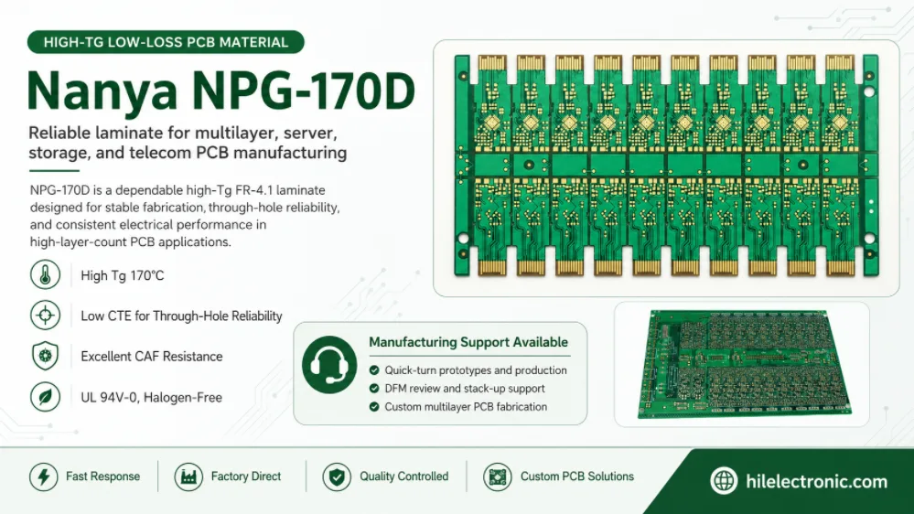
Nanya NPG-170D PCB for Halogen-Free High-Tg Builds
“NPG-170D” is a family-level shorthand, not a complete...

Panasonic MEGTRON 7N PCB for AI Server HDI Boards
Panasonic MEGTRON 7N is best understood as a platform...

Ventec VT-481 PCB for Lead-Free Reliability
Ventec VT-481 is a mid-Tg, phenolic-cured FR-4.0 laminate...

TUC TU-872 SLK PCB for High-Speed FR-4 Cost Control
TUC TU-872 SLK occupies a commercially useful middle...
How to get a quote for PCBs
Let us run DFM/DFA analysis for you and get back to you with a report.
You can upload your files securely through our website.
We require the following information in order to give you a quote:
-
- Gerber, ODB++, or .pcb, spec.
- BOM list if you require assembly
- Quantity
- Turn time
In addition to PCB manufacturing, we offer a comprehensive range of electronic services, including PCB design, PCBA (Printed Circuit Board Assembly), and turnkey solutions. Whether you need help with prototyping, design verification, component sourcing, or mass production, we provide end-to-end support to ensure your project’s success. For PCBA services, please provide your BOM (Bill of Materials) and any specific assembly instructions. We also offer DFM/DFA analysis to optimize your designs for manufacturability and assembly, ensuring a smooth production process.