
Highleap Electronic: Leading Telecom PCB Manufacturer

In today’s hyper-connected world, the backbone of seamless communication lies in the sophisticated hardware that powers our telecommunication systems. At the heart of these systems are Telecom PCBs, essential components that ensure reliable and efficient signal transmission. Highleap Electronic, a leading PCB manufacturing and assembly provider, specializes in delivering high-quality telecommunication circuit boards tailored to meet the evolving demands of the telecom industry.
What Are Telecom PCBs?
Telecom PCBs are specialized circuit boards designed to support the complex functionalities of telecommunication devices and infrastructure. These boards serve as the foundation for various components, including processors, memory modules, and signal transceivers, enabling the seamless flow of data and voice signals across networks. Also known as telecommunication printed circuit boards or telecom circuit boards, these PCBs are engineered to handle high-frequency signals and ensure minimal interference and signal loss.
Importance of Telecom PCBs in Communication Networks
The efficiency and reliability of communication networks heavily depend on the quality of telecom PCBs. Here’s why they are indispensable:
High Performance: Telecom PCBs are designed to support high-speed data transmission, which is crucial for applications like 5G networks, fiber optics, and satellite communications.
Durability: These PCBs must withstand harsh environmental conditions, including extreme temperatures, moisture, and electromagnetic interference, ensuring long-term performance.
Compact Design: With the increasing demand for miniaturization in telecom devices, telecommunication circuit boards are crafted to maximize functionality within a limited space, enhancing the overall efficiency of the devices.
Scalability: Telecom PCBs are adaptable to various scales, from small mobile devices to large-scale network infrastructure, providing flexibility for expanding communication systems.

Telecommunication Equipment and Their PCB Types
Telecommunication systems comprise a diverse array of equipment, each necessitating specific types of PCBs to ensure optimal performance and reliability. Understanding the intricate relationship between telecommunication devices and their corresponding PCB technologies is essential for designing efficient and robust communication networks. Highleap Electronic excels in providing specialized PCB solutions tailored to the unique requirements of various telecommunication equipment, ensuring seamless connectivity and superior signal integrity.
Base Transceiver Stations (BTS), Routers, and Switches are fundamental components of cellular and networking infrastructures. BTS units, which facilitate wireless communication between user devices and the broader network, rely on Multi-Layer High-Frequency PCBs to manage high-frequency signals with minimal loss and interference. Similarly, routers and switches, which handle vast amounts of data traffic, utilize High-Density Interconnect (HDI) PCBs. HDI PCBs offer the necessary routing complexity and compactness to support multiple high-speed data pathways within limited spaces, ensuring efficient data management and network performance.
Optical Network Terminals (ONTs), Satellite Communication Systems, and 5G Infrastructure Equipment represent the cutting edge of modern telecommunication technologies. ONTs, responsible for converting fiber optic signals into electrical signals for home and business networks, benefit from Flexible PCBs (FPCs) due to their ability to bend and fit into confined spaces, enhancing reliability and signal transmission. Satellite communication systems demand Rigid-Flex PCBs that can withstand the extreme vibrations and thermal variations encountered in space environments, providing the durability and flexibility necessary for consistent performance. The advent of 5G technology has introduced a need for High-Speed Digital PCBs, designed with precise impedance control and superior signal integrity features to support ultra-fast data rates and low latency, essential for next-generation communication networks.
Fiber Optic Transceivers and Wireless Access Points (WAPs) further illustrate the specialized PCB requirements within telecommunication systems. Fiber optic transceivers, which convert electrical signals to optical signals and vice versa, utilize Microstrip PCBs for their capability to handle high-frequency radio frequency (RF) signals with exceptional signal integrity. On the other hand, WAPs, which distribute wireless signals within localized areas, employ Single-Layer or Dual-Layer PCBs depending on their complexity and feature set. Single-layer PCBs offer cost-effective solutions for simpler WAPs, while dual-layer PCBs provide enhanced performance and connectivity for more advanced wireless access points. By leveraging these specialized PCB types, Highleap Electronic ensures that each piece of telecommunication equipment operates at peak efficiency, supporting the ever-growing demands of global communication networks.

Key Features of Highleap Electronic’s Telecom PCBs
At Highleap Electronic, we recognize that telecom PCBs are critical to the performance and reliability of modern communication systems. Our expertise in PCB manufacturing and assembly ensures that we deliver telecommunication circuit boards tailored to meet the specific needs of our clients. Here are the standout features of our telecom PCBs that provide significant value to your projects:
-
-
Customer-Specified Materials for Optimal Performance
Understanding that each telecom application has unique requirements, Highleap Electronic offers flexibility in PCB material selection. While clients typically specify the substrates and materials based on their performance criteria, our team provides expert guidance to ensure the chosen materials are compatible with the intended application. Whether you require high-frequency substrates like PTFE for RF applications or durable materials for rugged environments, we accommodate your specifications to achieve optimal signal integrity and thermal management tailored to your project’s demands. -
Advanced Manufacturing Techniques for Precision and Reliability
Our state-of-the-art manufacturing facilities are equipped with the latest technologies, including laser direct imaging (LDI), automated optical inspection (AOI), and controlled impedance routing. These advanced processes enable us to produce multi-layer PCBs with precise etching, drilling, and layering, essential for high-density and high-frequency telecom applications. Additionally, our stringent manufacturing protocols ensure consistent quality and reliability, making our PCBs suitable for critical infrastructure such as 5G base stations, satellite communication systems, and high-speed networking equipment. -
Comprehensive Quality Assurance and Testing
Highleap Electronic is committed to delivering defect-free telecom PCBs that meet international standards. Our rigorous quality assurance processes include multi-stage inspections, electrical testing, thermal cycling, and impedance analysis to verify each PCB’s performance under real-world conditions. We adhere to industry certifications such as ISO 9001 and IPC-6012, ensuring that our products not only meet but exceed the expectations of our clients. By maintaining high standards of quality, we ensure that your telecommunication equipment operates reliably and efficiently, minimizing downtime and enhancing overall system performance.
-
By prioritizing customer specifications, leveraging advanced manufacturing technologies, and maintaining comprehensive quality assurance, Highleap Electronic delivers telecom PCBs that drive the success of your communication systems. Partner with us to benefit from our expertise and commitment to excellence, ensuring your telecommunication projects achieve their highest potential.
Why Choose Highleap Electronic for Your Telecom PCB Needs?
Highleap Electronic stands out as a premier provider of telecom PCBs and assembly services for several reasons:
-
-
Expertise and Experience: With years of experience in the PCB manufacturing industry, we possess the technical knowledge and skills to handle even the most complex telecom projects.
-
Cutting-Edge Technology: Our investment in the latest manufacturing equipment and software ensures precision and efficiency in every PCB we produce.
-
Customer-Centric Approach: We prioritize our clients’ needs, offering personalized solutions and responsive support to ensure your project’s success.
-
Competitive Pricing: Highleap Electronic delivers top-quality telecommunication circuit boards at competitive prices, providing excellent value without compromising on quality.
-
Conclusion
In the realm of telecommunications, the quality and reliability of PCBs are crucial to maintaining robust and efficient communication networks. Telecom PCBs are the unsung heroes that facilitate seamless connectivity, and choosing the right manufacturing partner is essential. Highleap Electronic offers unparalleled expertise in PCB manufacturing and assembly, ensuring that your telecommunication systems operate at their best. From base transceiver stations to 5G infrastructure equipment, our diverse range of telecommunication printed circuit boards caters to various devices and applications, driving your business forward.
Contact us today to learn how our telecommunication printed circuit boards can enhance your communication solutions and drive your business forward.
Frequently Asked Questions (FAQ)
1. What Certifications Ensure High-Quality Telecom PCBs?
When selecting a PCB manufacturer for telecommunication applications, certifications are crucial indicators of quality and reliability. Highleap Electronic adheres to internationally recognized standards such as ISO 9001 for quality management systems and IPC-6012 for rigid printed boards and other forms of component mounting or interconnecting structures. Additionally, our PCBs comply with RoHS directives, ensuring they are free from hazardous substances. These certifications guarantee that our telecom PCBs meet stringent industry requirements, providing you with dependable and high-performance solutions.
2. Can Highleap Electronic Assist with PCB Design for Telecom Applications?
Yes, Highleap Electronic offers comprehensive design support services to help you develop optimized PCB layouts tailored to your specific telecommunication needs. Our team of experienced engineers collaborates closely with clients to ensure that every aspect of the PCB design—from layer configuration and component placement to signal integrity and thermal management—is meticulously planned and executed. Whether you require assistance with high-frequency design, multi-layer configurations, or specialized connector placements, we provide the expertise necessary to bring your telecom projects to fruition efficiently and effectively.
3. What Are the Typical Lead Times for Manufacturing Telecom PCBs?
Lead times for manufacturing telecom PCBs can vary based on factors such as complexity, layer count, volume, and specific client requirements. Highleap Electronic is committed to delivering timely solutions without compromising on quality. For standard telecom PCB projects, our typical lead time ranges from 1 to 2 weeks from the date of order confirmation. For more complex or high-volume orders, we work closely with clients to establish realistic timelines and ensure on-time delivery. Our streamlined manufacturing processes and efficient supply chain management enable us to meet tight deadlines and support your project schedules effectively.
4. How Does Highleap Electronic Handle Quality Control for Telecom PCBs?
Quality control is a paramount aspect of Highleap Electronic’s manufacturing process. We implement a multi-tiered quality assurance system that includes:
-
- Automated Optical Inspection (AOI): Detects surface defects and ensures accurate component placement.
- Electrical Testing: Verifies the functionality of each PCB through in-circuit testing (ICT) and flying probe tests.
- Thermal Cycling: Assesses the PCB’s durability under varying temperature conditions to simulate real-world operational environments.
- Impedance Analysis: Ensures signal integrity for high-frequency applications.
- Final Visual Inspections: Conducted by experienced technicians to identify any remaining defects. By rigorously adhering to these quality control measures, we ensure that every telecom PCB leaving our facility meets the highest standards of performance and reliability.
5. What Options Are Available for PCB Assembly Services?
Highleap Electronic provides comprehensive PCB assembly services to complement our manufacturing capabilities. Our assembly options include:
-
- Surface Mount Technology (SMT): Ideal for high-density and high-frequency components used in telecom PCBs.
- Through-Hole Technology (THT): Suitable for components that require robust mechanical connections.
- Mixed Technology Assembly: Combines SMT and THT to accommodate a wide range of component types and sizes.
- Box Build Assembly: Complete assembly of the entire device, including mounting, wiring, and final packaging. Additionally, we offer custom packaging solutions, inventory management, and kitting services to streamline your supply chain and ensure seamless integration of our PCBs into your final products. Our flexible assembly services are designed to meet the diverse needs of the telecommunications industry, providing you with turnkey solutions that enhance efficiency and reduce time-to-market.
Get a Free PCB & PCBA Quote

Recommended Posts
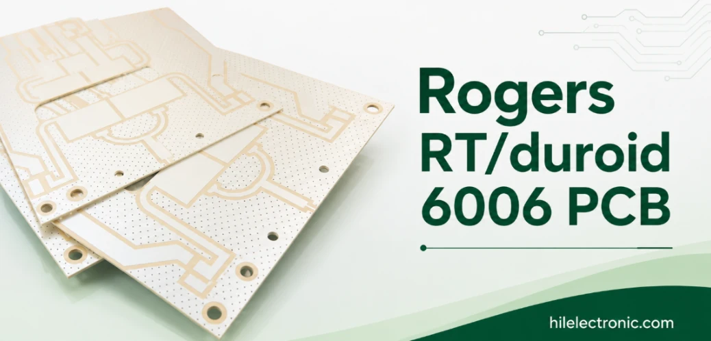
RT/duroid 6006 PCB Manufacturer for Compact High-Dk Microwave Circuits
RT/duroid 6006 is selected when circuit area is expensive....
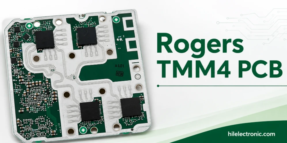
Rogers TMM4 PCB Manufacturer for Compact Microwave Filters
TMM4 is most useful when a microwave circuit must become...
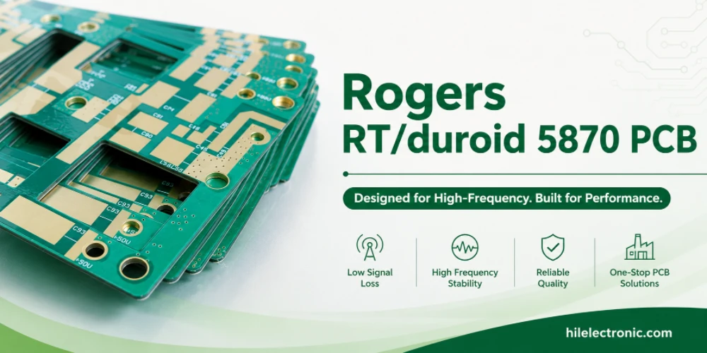
RT/duroid 5870 PCB Manufacturer for Low-Loss PTFE RF Circuits
RT/duroid 5870 is chosen when the RF path needs low loss,...
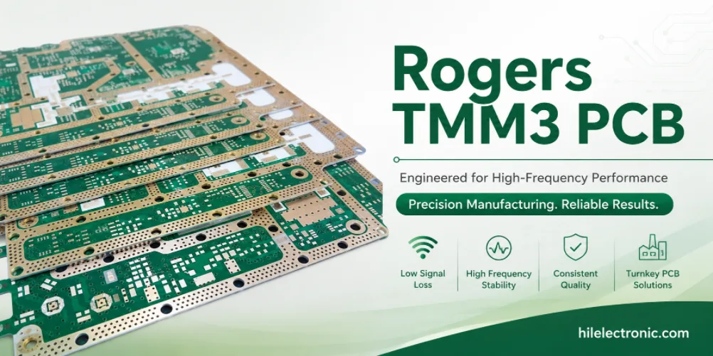
Rogers TMM3 PCB Manufacturer for Mechanical RF Modules
TMM3 is selected when an RF circuit must behave as part of...
How to get a quote for PCBs
Let us run DFM/DFA analysis for you and get back to you with a report.
You can upload your files securely through our website.
We require the following information in order to give you a quote:
-
- Gerber, ODB++, or .pcb, spec.
- BOM list if you require assembly
- Quantity
- Turn time
In addition to PCB manufacturing, we offer a comprehensive range of electronic services, including PCB design, PCBA (Printed Circuit Board Assembly), and turnkey solutions. Whether you need help with prototyping, design verification, component sourcing, or mass production, we provide end-to-end support to ensure your project’s success. For PCBA services, please provide your BOM (Bill of Materials) and any specific assembly instructions. We also offer DFM/DFA analysis to optimize your designs for manufacturability and assembly, ensuring a smooth production process.