
PCB Copper Roughness: Signal Loss, Material Selection and Manufacturing Control
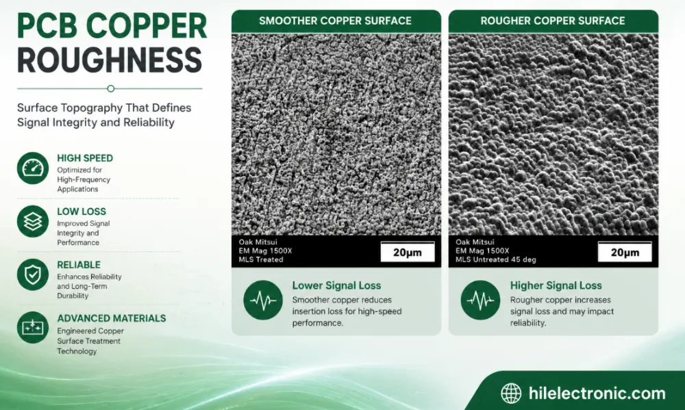
PCB copper roughness is the microscopic surface texture of copper foil and treated interfaces. At high frequency, current is concentrated near the conductor surface, so roughness increases the effective path length and conductor loss. It can also affect phase delay and the apparent impedance model.
Highleap Electronics does not manufacture copper foil. We procure and process the approved foil/laminate construction, manufacture the PCB and assemble the PCBA.
Does lower copper roughness always make a better PCB? Electrically, smoother copper usually reduces high-frequency conductor loss. Manufacturing still requires adequate adhesion, process compatibility, availability and qualification. The correct foil is a controlled trade-off, not a marketing label.
What Is PCB Copper Roughness?
Electrodeposited copper has a drum side and a treated side, and laminate suppliers may offer standard, reverse-treated, very-low-profile or hyper-very-low-profile constructions. Naming is not perfectly consistent across suppliers, so the released design should identify the exact foil or an approved roughness limit.
HTE / standard-profile copper
Strong adhesion and broad availability, but usually higher conductor loss.
RTF
Moves treatment to reduce the rough surface seen by the signal, depending on construction.
VLP
Lower profile for improved high-frequency performance.
HVLP / advanced smooth foil
Used where 112G, 224G, mmWave or long channels justify additional cost and control.
For a buyer, the useful distinction is between the technology name and the finished-board requirement. The board still has to control interaction between roughness, resin and adhesion, base-foil profile, treated-side roughness and finished copper thickness. Highleap reads those requirements from the actual design data and converts them into a stackup, process route and inspection plan, rather than assuming that the keyword alone defines how the PCB should be built.
How Copper Roughness Affects PCB Performance
| Effect | Mechanism | Design consequence |
|---|---|---|
| Higher insertion loss | Longer effective current path at the rough surface | Reduced channel margin |
| Phase-delay change | Roughness changes effective inductive/capacitive behavior | Timing and model correlation error |
| Impedance-model error | Smooth-conductor model does not match production foil | Coupon and simulation mismatch |
| Greater heating | Increased AC resistance | Potential thermal impact in high-power RF paths |
| Lot variation | Different foil or treatment | Inconsistent insertion loss |
Generic datasheet values are not enough when ordinary electrical testing cannot detect unapproved substitution of a rougher foil or higher insertion loss than simulated. The review must use the exact core or prepreg, copper profile, finished thickness and via route. This is where one-to-one engineering support prevents the buyer from having to interpret multiple supplier documents alone.
Generic datasheet values are not enough when ordinary electrical testing cannot detect prototype-to-production variation or unapproved substitution of a rougher foil. The review must use the exact core or prepreg, copper profile, finished thickness and via route. This is where one-to-one engineering support prevents the buyer from having to interpret multiple supplier documents alone.
When Copper Roughness Becomes Critical
- Long 56G, 112G or 224G electrical channels.
- 800G and 1.6T optical-module host or module boards.
- 77 GHz radar and mmWave antenna/feed structures.
- Low-loss laminate designs where conductor loss is a large share of total loss.
- Thin traces or narrow geometries with high current concentration.
- Designs requiring correlation between simulation and S-parameter measurement.
Repeatability is the main manufacturing test. A prototype can work even when the process window is broad, but volume production exposes variation in material lots, copper distribution, panel loading and plating. We place finished-copper control, coupon correlation to the released model, supplier foil verification and material lot traceability in the production release to provide a stable comparison between lots.
Repeatability is the main manufacturing test. A prototype can work even when the process window is broad, but volume production exposes variation in material lots, copper distribution, panel loading and plating. We place coupon correlation to the released model, supplier foil verification, material lot traceability and finished-copper control in the production release to provide a stable comparison between lots.
Copper Roughness Data and Modeling
RMS roughness alone may not fully describe the surface. Models such as Hammerstad, Huray and multi-level approaches use different parameters. The designer and manufacturer should agree which foil surface and data are represented.
Common errors include modeling the laminate side while the signal sees a different surface, using a generic VLP value, or ignoring plated copper added during fabrication.
The output of the review should be a buildable stackup and a short list of controlled variables. Highleap documents the agreed material identity, geometry, process route and inspection basis, then coordinates the remaining details internally across CAM, fabrication, quality and assembly.
The technical variables in this section cannot be evaluated independently. A change in treated-side roughness can alter the effect of finished copper thickness, while interaction between roughness, resin and adhesion and base-foil profile influence the geometry and test result seen on the finished board. Highleap reviews the actual production construction so the stackup and compensation are based on purchasable materials rather than nominal examples.
Electrical Loss Versus Copper Adhesion
The rough treatment helps copper bond to the dielectric. Excessively smooth foil without a qualified resin/treatment system can reduce peel strength or process robustness. Modern laminate systems use chemical treatments and resin design to achieve adhesion with lower profile.
Highleap does not remove or polish copper treatment after lamination. The correct solution is to order a qualified copper-clad construction from the material supplier.
Design intent and factory compensation have different owners. The customer defines electrical and reliability requirements; Highleap applies the approved CAM, drilling, plating and lamination adjustments needed to reach the finished values. Any change that affects architecture or qualification is raised for approval instead of being hidden inside CAM processing.
The correct balance is achieved through a qualified laminate-and-foil construction, not by asking the PCB factory to remove the treatment that provides adhesion. Resin chemistry, chemical treatment and foil profile are designed as a system. Highleap verifies the approved construction and processing route, then controls finished copper and geometry. Any move to a smoother foil should be evaluated for both electrical benefit and mechanical qualification.
Implications of Leaving Copper Type Unspecified
- The factory may quote a standard foil that does not match the channel model.
- A material substitution can preserve resin Dk/Df but change conductor loss.
- Prototype and production lots may use different available foil.
- Insertion-loss coupons may fail even though impedance passes.
- RF structures can shift because roughness changes loss and effective electrical length.
The serious failures usually appear after components have been assembled. A board may pass continuity and still show higher insertion loss than simulated, phase-delay mismatch or prototype-to-production variation during system validation. Early DFM is therefore less expensive than investigating a finished PCBA, because material, geometry, fabrication and assembly causes can still be separated before tooling and component placement.
Repeat production creates another risk: a later lot can use a different available construction while the nominal material family remains unchanged. Highleap records the approved stackup, copper, process assumptions and inspection method so prototypes and production are compared against the same release basis.
How Highleap Controls Copper Roughness in Production
- Verify the laminate and foil designation with the supplier.
- Record copper type, base weight and finished copper in the stackup.
- Use artwork compensation matched to copper thickness and process.
- Control plating so finished geometry and copper remain within the model.
- Keep material substitutions under customer change control.
- Use representative impedance and loss coupons when specified.
- Correlate production data to the released simulation assumptions.
The approved manufacturing data are retained for repeat orders. Material identity, scaling, drill route, plating target and inspection method remain under change control. This protects the product from unapproved substitution of a rougher foil or higher insertion loss than simulated caused by an undocumented process or supply change.
A capability claim has value only when it is connected to a controlled shop-floor route. Highleap links material lot traceability, finished-copper control, coupon correlation to the released model and supplier foil verification to incoming inspection, lamination, drilling, plating, imaging and final verification. The exact sequence remains subject to the approved material and board construction.
Highleap High-Speed PCB Fabrication and Assembly
Highleap supports low-loss and ultra-low-loss material systems, low-profile copper, controlled impedance, fine-line etching, HDI, back drilling, AOI, cross-section and optional S-parameter/insertion-loss tests. PCBA services include SPI, BGA assembly, AOI, X-ray, connectors and functional test.
The assembly process begins with the bare-board construction. Warpage, copper balance, pad finish, via condition and thermal mass influence printing, placement and reflow. Highleap reviews the PCB and component layout together so a board that meets bare-board tests does not become a low-yield PCBA after high-value parts are loaded.
One project engineer coordinates fabrication and SMT questions. This avoids a common failure in which the PCB is optimized without considering assembly, or the assembly plan assumes pad, warpage and thermal conditions that the bare-board construction cannot reliably provide.
Copper roughness control begins before fabrication because the foil is supplied as part of the copper-clad laminate. During production, plating and etching still change conductor thickness and shape, so the finished trace must remain consistent with the model. On assembled boards, launches, pads and component transitions may dominate local discontinuity even when the long routed section uses smooth copper. The review therefore covers both PCB and PCBA interfaces.
Send the PCB Design First; We Will Confirm the Copper Requirement
Purchasing does not need to select a copper-roughness model before requesting a quote. Send the Gerber files or PCB design files first. If copper or material notes are already included, no separate roughness specification is needed for the initial review.
Our engineers connect electrical intent with available production material
A dedicated Highleap engineer will review the routing, frequency range and material construction with our high-speed manufacturing team. We will confirm whether standard copper, VLP, HVLP or another approved profile should be discussed, and we will contact you directly if supplier data or customer approval is required.
The assigned engineer keeps all communication in one project path. Material, stackup, CAM, fabrication, quality and assembly questions are consolidated so the buyer does not have to route technical issues between multiple factory departments.
Copper Roughness Cost Factors
VLP/HVLP foil can increase laminate cost and reduce sourcing flexibility. Tight foil control may extend lead time. The cost should be justified by channel analysis; specifying the smoothest available copper on noncritical layers is usually unnecessary.
The quotation reflects the complete route required to achieve acceptable yield. Major drivers include VLP or HVLP availability, approved material constructions, copper weight, sourcing lead time and required loss testing. Material price is only one component; extra lamination, special drilling, tight registration, inspection time and test coupons can have an equal or larger effect.
Lead time is often controlled by material availability, special copper, supplier minimums, sequential processing or outside characterization. The engineer identifies the actual schedule constraint and checks whether an approved alternative can remove it without changing the product requirement.
Specifying VLP or HVLP on every layer can increase material cost without improving the noncritical portions of the design. Some constructions are available only in selected thicknesses, copper weights or supplier regions, which can also affect lead time and minimum order quantities. Highleap can help identify which layer pairs are loss-critical and whether the approved material family offers a practical smoother-copper construction.
Copper Is Part of the Material System and the Channel Model
A low-Df laminate with uncontrolled copper is not a controlled high-speed PCB. Highleap makes the ordered foil, plating, geometry and test plan part of the manufacturing release.
Generic datasheet values are not enough when ordinary electrical testing cannot detect phase-delay mismatch or prototype-to-production variation. The review must use the exact core or prepreg, copper profile, finished thickness and via route. This is where one-to-one engineering support prevents the buyer from having to interpret multiple supplier documents alone.
The resin system, glass style and copper profile should be released together. Changing only the foil can alter insertion loss, phase delay, adhesion behavior and material availability even when the laminate family name remains unchanged. For repeat production, Highleap records the exact purchased construction and treats a copper-profile change as a controlled substitution rather than a routine purchasing decision.
Frequently Asked Questions
What is the difference between VLP and HVLP copper?
Both describe low-profile foil categories, but naming and limits vary by supplier. Specify the exact foil or roughness data.
Does smoother copper reduce PCB loss?
Usually yes at high frequency, but the complete conductor geometry, plating, adhesion and dielectric system still matter.
Can Highleap measure copper roughness?
Material certification and supplier data are the normal controls. Specialized surface metrology can be discussed if contractually required.
Does surface finish matter more than copper roughness?
Both can matter, but base-foil roughness often affects the full trace length while finish affects exposed areas and pads.
Does Highleap manufacture copper foil?
No. We manufacture PCBs using approved copper-clad laminates and foil constructions.
Do I need to specify VLP or HVLP copper before contacting Highleap?
No. Send the Gerber files or PCB design files first. A Highleap engineer will review the channel and material construction with our technical team and confirm whether a specific copper profile is needed.
Technical reference note: Material properties and interface descriptions must be checked against the current manufacturer datasheet, customer specification and applicable interface standard for the exact production construction. Highleap Electronics is the PCB fabrication and PCB assembly provider; laminate and component trademarks belong to their respective manufacturers.

Recommended Posts

TMM4 Filter PCB Manufacturing
TMM4 filter PCB manufacturing is controlled by the...

TMM3 PCB Manufacturing for RF Modules
TMM3 PCB manufacturing is most useful where the RF module...

TMM6 PCB Fabrication
TMM6 fabrication is the process-control page for a mid-Dk...

TMM10 PCB Manufacturing for Compact RF Designs
Table of contentsHow TMM10 Shrinks RF StructuresTMM10 vs...
How to get a quote for PCBs
Let’s run DFM/DFA analysis for you and get back to you with a report. You can upload your files securely through our website. We require the following information in order to give you a quote:
-
- Gerber, ODB++, or .pcb, spec.
- BOM list if you require assembly
- Quantity
- Turn time
For PCBA services, please provide your BOM (Bill of Materials) and any specific assembly instructions. We also offer DFM/DFA analysis to optimize your designs for manufacturability and assembly, ensuring a smooth production process.