
Understanding Signal Transmission in High Frequency PCBs

Introduction
In conventional low-frequency circuits, signals are typically treated as simple voltage variations moving through conductors. However, as operating frequencies increase into the gigahertz range, signal behavior fundamentally changes. High frequency signal transmission exhibits electromagnetic wave characteristics rather than simple voltage propagation, introducing complexities such as reflections, crosstalk, and frequency-dependent losses. Modern applications in telecommunications, radar systems, and high-speed computing demand precise control over how signals propagate through printed circuit boards to maintain system performance.
How High Frequency Signal Transmission Works in PCBs
1. From Low Frequency to High Frequency Behavior
At low frequencies where circuit dimensions remain much smaller than the signal wavelength, designers can ignore transmission line effects and apply simple circuit laws. As frequency increases, wavelengths become comparable to PCB trace lengths, forcing consideration of wave propagation characteristics. High frequency signal transmission must account for the time delay as electromagnetic energy travels along conductors, making transmission line theory essential. This transition typically becomes critical when signal rise times drop below one nanosecond or frequencies exceed 1 GHz.
2. Role of Transmission Lines
Transmission lines in PCB design serve as controlled paths for electromagnetic wave propagation. The characteristic impedance (Z₀) represents the ratio of voltage to current for a traveling wave and depends on trace geometry and dielectric properties. Microstrip configurations place signal traces on outer layers with reference planes below, while stripline structures sandwich signals between two reference planes. The relationship between the signal trace and its reference plane determines the electromagnetic field distribution, directly affecting how high frequency signal transmission maintains integrity across the board.
Key Factors Affecting High Frequency Signal Transmission
1. PCB Material Properties
The dielectric constant (Dk) determines signal propagation velocity, while loss tangent (Df) quantifies energy dissipation as heat during transmission. Standard FR4 materials perform adequately below 5 GHz but show significant losses at higher frequencies. Advanced materials like Rogers laminates or PTFE-based substrates provide stable dielectric properties and minimal loss factors essential for demanding applications. Material selection directly impacts achievable bandwidth, signal attenuation, and design margins.
2. Trace Geometry and Impedance Control
Trace width, thickness, and spacing relative to reference planes establish the characteristic impedance of transmission lines. Maintaining consistent geometry throughout signal paths prevents impedance discontinuities that generate reflections and degrade high frequency signal transmission performance. The coupling strength between signal traces and reference planes fundamentally determines waveform fidelity preservation across the PCB structure.
3. Return Path and Grounding
Every signal current requires a return path that ideally mirrors the signal trace directly beneath it on an adjacent reference plane. Breaks or interruptions in the return path force current detours, creating loop inductance that degrades signal quality and increases electromagnetic emissions. Multi-layer stackups with dedicated ground planes provide low-impedance return paths, while strategic via placement near layer transitions maintains return path continuity for reliable high frequency signal transmission.
4. Via and Discontinuity Effects
Vias create impedance discontinuities through their parasitic capacitance and inductance, causing partial signal reflections. Via stubs—unused portions of plated through-holes extending beyond the signal layer—act as resonant structures that severely degrade performance above 5 GHz. Back-drilling to remove stubs, using blind or buried vias, and optimizing pad geometries minimize these effects on high frequency signal transmission integrity.

High-frequency PCBs
Common Issues in High Frequency Signal Transmission
Signal reflection occurs when impedance mismatches exist along transmission paths, causing portions of transmitted energy to reflect back toward the source. These reflections create standing waves, overshoot, and ringing that can trigger false logic states. Proper termination strategies—series, parallel, or AC termination—match impedances to minimize reflections:
- Series termination – Places resistor at source to match driver impedance, suitable for point-to-point connections
- Parallel termination – Connects resistor to supply or ground at receiving end, effective for multiple loads
- AC termination – Uses RC network to minimize reflections while reducing DC power consumption
Crosstalk develops when electromagnetic coupling between adjacent traces allows signals to induce unwanted voltages on neighboring conductors. Increasing trace separation, utilizing differential signaling, and placing ground traces between critical signals effectively control crosstalk in high frequency signal transmission designs.
Impedance mismatch between different signal path sections—traces, vias, connectors, or components—accumulates across multiple transitions and significantly impacts performance. Even 5-10% impedance variations can cause measurable degradation above 10 GHz, requiring tight manufacturing tolerances.
Design Practices to Improve High Frequency Signal Transmission
Controlled impedance design begins during stackup planning and continues through trace routing. Field solver tools calculate required trace dimensions for specified impedances—typically 50 ohms single-ended or 100 ohms differential—accounting for dielectric properties, copper weights, and fabrication tolerances. This systematic approach ensures high frequency signal transmission meets performance targets.
Low-loss dielectric materials appropriate for the application’s frequency range directly improve signal amplitude preservation. While premium materials increase costs, they become necessary when operating above 10 GHz or when insertion loss budgets are constrained:
- Standard FR4 – Adequate for frequencies below 5 GHz, Dk ~4.2-4.5, Df ~0.02
- Mid-loss materials – Rogers RO4350B for 5-20 GHz applications, Dk ~3.48, Df ~0.0037
- Low-loss materials – Rogers RO3003 or PTFE-based for above 20 GHz, Dk ~3.0, Df ~0.001
Signal integrity simulation using electromagnetic field solvers validates designs before fabrication. These tools predict impedance profiles, crosstalk levels, insertion loss, and time-domain waveforms under various operating conditions. Early simulation identifies issues when corrections require only design changes rather than expensive board respins, ensuring high frequency signal transmission performance meets specifications.
Return path continuity demands attention during layer stackup design and component placement. Signal layers should always reference adjacent planes without interruption:
- Solid reference planes – Avoid splits beneath high-speed traces to maintain return current paths
- Layer transitions – Place ground vias adjacent to signal vias when changing layers
- Plane changes – Use stitching vias to connect reference planes when signals cross plane types
Ensuring continuous return paths minimizes electromagnetic interference and preserves signal integrity across high-frequency PCB designs.
Conclusion
High frequency signal transmission represents electromagnetic wave propagation requiring rigorous impedance control, careful return path management, and understanding of material and geometric factors affecting signal integrity. These principles form the foundation for reliable RF circuits, high-speed digital interfaces, and advanced communication systems operating at multi-gigahertz frequencies.
At Highleap Electronics, our engineering team provides expertise in controlled impedance design and high-frequency PCB manufacturing, helping ensure optimal signal integrity for complex electronic systems. Contact us to discuss how our capabilities can support your next high-frequency design challenge.

Recommended Posts
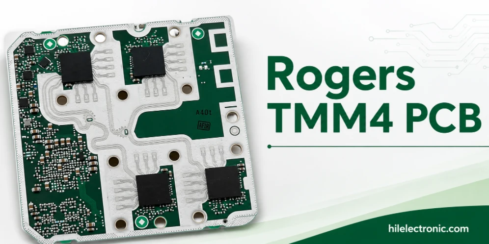
Rogers TMM4 PCB Manufacturer for Compact Microwave Filters
TMM4 is most useful when a microwave circuit must become...
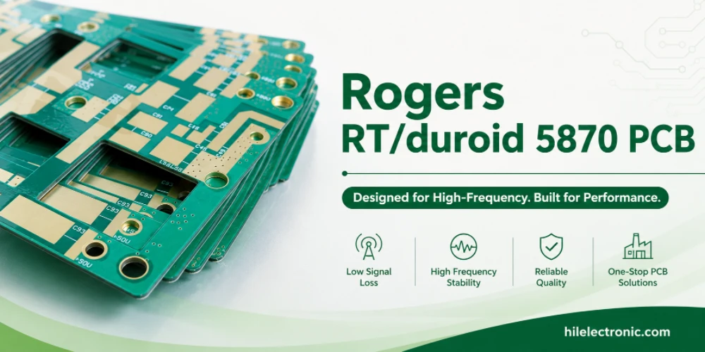
RT/duroid 5870 PCB Manufacturer for Low-Loss PTFE RF Circuits
RT/duroid 5870 is chosen when the RF path needs low loss,...
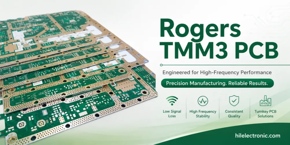
Rogers TMM3 PCB Manufacturer for Mechanical RF Modules
TMM3 is selected when an RF circuit must behave as part of...
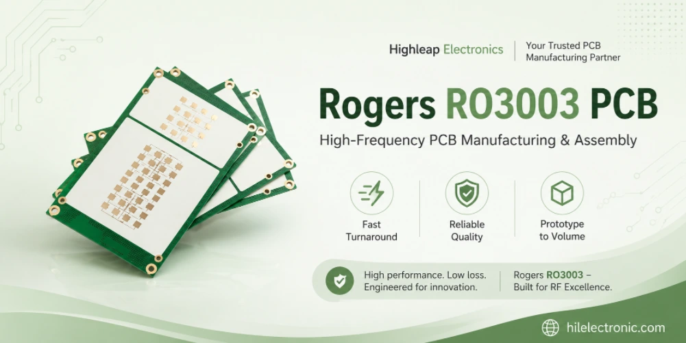
Rogers RO3003 PCB Manufacturer for Automotive Radar and mmWave Modules
A 77 GHz radar board is purchased as a working sensor...
How to get a quote for PCBs
Let‘s run DFM/DFA analysis for you and get back to you with a report. You can upload your files securely through our website. We require the following information in order to give you a quote:
-
- Gerber, ODB++, or .pcb, spec.
- BOM list if you require assembly
- Quantity
- Turn time
In addition to PCB manufacturing, we offer a comprehensive range of electronic services, including PCB design, PCBA, and turnkey solutions. Whether you need help with prototyping, design verification, component sourcing, or mass production, we provide end-to-end support to ensure your project’s success.
For PCBA services, please provide your BOM (Bill of Materials) and any specific assembly instructions. We also offer DFM/DFA analysis to optimize your designs for manufacturability and assembly, ensuring a smooth production process.