
Back to blog
Controlled Impedance Requirements | PCB Impedance

Introduction
Controlled impedance is the cornerstone of high-performance PCB (Printed Circuit Board) design. It involves the precise regulation of a circuit’s resistance to alternating current, considering both resistance and reactance within the circuit. This crucial parameter plays a pivotal role in ensuring the proper functioning of circuits, affecting timing, integrity, and overall performance. In this comprehensive guide, we delve into the intricacies of controlled impedance, its significance in PCB design, and the factors that influence it.
Understanding Controlled Impedance
Controlled impedance, measured in Ohms (Ω), defines the resistance to alternating current in a PCB. It’s a critical consideration in designing high-frequency analog and high-speed digital circuits. The impedance of a circuit must be carefully managed during design to prevent signal distortion, reflection, and other issues that can disrupt proper functioning.
Impedance control is especially crucial when transitioning from lower impedance environments to higher impedance environments, as these transitions can lead to energy reflections capable of disrupting energy flow and causing circuit failures.
The Role of PCB Transmission Lines
To comprehend controlled impedance, one must understand PCB transmission lines. These lines are pathways that transmit signals from a PCB’s transmitters to its receivers. They consist of at least two conductors, typically a signal trace and a return path, often a ground plane, separated by dielectric material. Impedance control becomes essential when dealing with high-frequency signals traveling over PCB transmission lines.
Types of PCB Transmission Lines
PCB transmission lines are used to carry electrical signals from one point to another on the board while maintaining controlled impedance. Different types of PCB transmission lines are used depending on the specific requirements of the circuit and the application. Here are some common types of PCB transmission lines:
- Microstrip Line: Microstrip transmission lines are one of the most widely used types. They consist of a conductor trace on the top layer of the PCB, separated by a dielectric material from a ground plane on the bottom layer. The signal propagates along the conductor trace, and the ground plane provides a return path. Microstrip lines are commonly used in single-layer and multilayer PCBs.
- Stripline: Stripline transmission lines have a conductor trace sandwiched between two layers of dielectric material, with ground planes on both the top and bottom layers. The signal travels through the conductor trace, and the ground planes on either side provide a controlled path for the return current. Stripline configurations are typically used in multilayer PCBs.
- Coaxial Cable: While not a PCB-specific transmission line, coaxial cables can be used within PCB designs when precise impedance control is required. Coaxial cables consist of an inner conductor, dielectric material, and an outer conductor or shield. They provide excellent shielding against external interference and are suitable for RF and high-frequency applications.
- Coplanar Waveguide (CPW): Coplanar waveguides are transmission lines where the signal conductor is surrounded by ground planes on either side, but there is no dielectric material above or below the conductor. CPW lines are often used in RF and microwave applications due to their controlled impedance characteristics.
- Differential Pair: A differential pair consists of two conductors running parallel to each other with a controlled separation distance. These pairs are used for high-speed data transmission and are commonly found in applications like USB, HDMI, and Ethernet connections. Maintaining controlled impedance in differential pairs is crucial to minimize signal skew and crosstalk.
- Edge-Coupled Microstrip: Edge-coupled microstrip lines are microstrip traces that run parallel to each other with a small separation distance. They are commonly used for differential signaling and RF applications.
- Slotline: Slotline transmission lines involve a conductor trace placed within a slot in the ground plane. The slot acts as a waveguide, and the signal propagates within it. Slotlines are less common but find use in specific applications.
The choice of transmission line type depends on factors such as the frequency of operation, signal integrity requirements, available board real estate, and design constraints. Designers select the appropriate transmission line configuration to ensure controlled impedance and reliable signal transmission for their specific PCB designs.
Factors Affecting Impedance Control in PCB Design
Several factors influence impedance control during PCB design, including:
- Trace Width: The width of the copper trace on a PCB affects impedance. Wider traces result in lower impedance, and trace width is chosen based on design considerations and impedance requirements.
- Copper Thickness: The thickness of the copper on the PCB impacts impedance. Thicker copper leads to lower impedance, and adjusting copper thickness can help achieve desired impedance values.
- Dielectric Thickness: The thickness of the insulating material between traces plays a role in impedance. Thicker dielectric material tends to produce modest increases in impedance, while reducing it requires a significant reduction in thickness.
- Dielectric Constant (Er): The dielectric constant represents the material’s ability to store electrical energy relative to a vacuum. Materials with low, stable dielectric constants are suitable for high-frequency applications and controlled impedance.
When Controlled Impedance Matters Most
Controlled impedance becomes paramount in scenarios characterized by transitions from lower to higher impedance environments. During such transitions, any impedance discontinuities can have profound effects, potentially leading to energy reflections and circuit disruptions. This significance is particularly pronounced in two key areas:
1. High-Powered Digital Devices: In high-powered digital devices, precise signal integrity is essential. These devices often involve the rapid transmission of digital signals with high data rates. Any impedance mismatches or disruptions in the transmission lines can result in signal distortion, reflections, and ultimately, errors in data communication. Controlling impedance ensures that signals propagate smoothly, maintaining the integrity of data transmission and preventing issues such as crosstalk and signal loss.
2. Radio Frequency (RF) Applications: RF applications operate at high frequencies, often involving wireless communication, radar systems, and microwave technology. In RF systems, maintaining controlled impedance is critical for efficient signal transmission and reception. Any impedance variations along transmission lines can lead to signal reflections that not only degrade signal quality but also result in the loss of transmitted energy. In sensitive RF applications like telecommunications, aerospace, and defense, maintaining impedance control is non-negotiable to ensure reliable and accurate communication.
In both these domains, controlled impedance not only facilitates efficient energy transfer but also minimizes electromagnetic interference (EMI) and ensures that signals arrive at their destinations with minimal distortion. Whether it’s high-powered digital devices or RF applications, the consequences of overlooking impedance control can be costly, leading to suboptimal performance, reduced reliability, and potentially compromised functionality. Therefore, in these contexts, meticulous attention to controlled impedance is a fundamental requirement to achieve the desired level of performance and operational reliability.
How Controlled Impedance Works
Controlled impedance in PCB design typically involves three levels of service:
- No Impedance Control: In situations with loose impedance tolerance, no specific design elements are needed for impedance control. This results in faster and more cost-effective board production.
- Impedance Watching: Designers outline impedance control requirements, and the PCB provider adjusts trace width and dielectric height accordingly. A Time-Domain Reflectometry (TDR) test may be performed to confirm impedance.
- Impedance Control: In cases where tight impedance tolerances are essential, manufacturers make the board and conduct a TDR test to ensure the desired impedance is achieved. Adjustments are made if necessary, and testing continues until the target impedance is reached.
Specifying PCB Impedance Control
To specify impedance control effectively, designers need to provide values for the target impedance, trace width, trace height, layer or layers for controlled traces, and spacing between copper components for coplanar or differential calculations. Clear and detailed documentation is essential to prevent delays and misunderstandings with fabricators.
Common Impedance Mistakes to Avoid
When specifying impedance control, it’s crucial to minimize errors to ensure project efficiency. Common mistakes to avoid include inconsistencies in trace width, failing to specify layers, setting unreasonable impedance targets, and discrepancies between notes and stackup information. Clear and accurate specifications prevent costly delays and ensure the successful completion of PCB projects.
Overall, controlled impedance is the linchpin of high-performance PCB design. Understanding its principles, factors influencing it, and how to specify it accurately is vital for achieving optimal circuit functionality. Whether in high-frequency analog circuits or high-speed digital applications, mastering controlled impedance is essential for designing PCBs that meet performance and reliability standards.
For production planning, it also helps to compare this topic with BGA PCB assembly and PCB conformal coating before finalizing the fabrication or assembly package.
PCB & PCBA Quick Quote
Related Articles
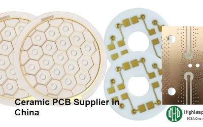
How to Choose a Ceramic PCB Supplier in China
How engineers source ceramic PCB suppliers in China without quality issues covering audits communication lead times and shipment control.
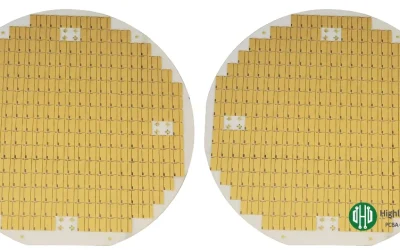
Ceramic PCB Supplier Evaluation for Electronics
A practical ceramic PCB supplier evaluation guide covering materials manufacturing processes certifications DFM support and turnkey assembly.
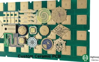
How to Specify Custom Ceramic PCB for Electronics
Learn how to specify a custom ceramic PCB for electronics including material selection copper bonding and thermal optimization.