
Design Guidelines for Copper Coin PCB: Thermal & Reliability Optimization

Introduction: Why Copper Coin PCB Design Matters in Power Electronics
Copper coin PCB technology has become essential in high-power and high-thermal-density circuits where conventional thermal management approaches cannot meet performance requirements. As power densities continue to increase in automotive electronics, LED lighting, and power conversion systems, embedded copper coin structures provide direct vertical heat conduction paths that dramatically reduce junction-to-case thermal resistance. The quality of copper coin PCB design directly determines both thermal performance and long-term reliability.
Understanding Embedded Copper Coin Structures
Core Structural Configurations
Embedded copper coin structures typically appear in three configurations: solid embedded copper blocks for concentrated heat sources, cylindrical copper posts for through-board thermal pathways, and copper bars for distributed power zones. Each configuration addresses specific thermal management requirements while maintaining mechanical integrity within the laminated board structure.
Thermal Conduction Pathways in Copper Coin PCB Design
The embedded copper coin creates a low-resistance thermal pathway connecting the component mounting surface directly to the heat sink or thermal base layer. Heat flows vertically from the device junction through the solder joint, into the surface copper pad, through the embedded copper coin, and finally to the bottom thermal interface. This vertical path bypasses the relatively poor thermal conductivity of standard FR-4 dielectric material, which typically exhibits thermal conductivity of only 0.3 to 0.4 W/mK compared to copper’s 400 W/mK.
Application-Specific Selection Criteria
High-power discrete semiconductors such as MOSFETs and IGBTs benefit most from solid copper blocks positioned directly beneath the device thermal pad. Multi-chip power modules often require multiple copper coins with optimized spacing to balance thermal distribution. Linear power zones in voltage regulator circuits may utilize copper bar configurations to spread heat across the regulated area effectively.

Copper Coin PCBs
Copper Coin Placement Strategy
Heat Source Alignment Principles
Successful copper coin PCB design requires precise alignment between the embedded copper structure and the component heat source. The copper coin must be positioned directly beneath the device thermal pad with minimal offset, typically maintaining alignment within 0.1 mm. Any misalignment introduces lateral thermal resistance through copper foil layers, significantly degrading thermal performance.
Multi-Device Layout Considerations
When multiple power devices operate in proximity, the copper coin PCB design must address several critical factors:
- Direct alignment with each heat source reduces thermal path resistance by 30 to 50 percent compared to offset placement.
- Maintain minimum 0.3 mm spacing between adjacent copper coins to prevent mechanical stress concentration during thermal cycling.
- Use symmetrical layout patterns for stress balance across the board, particularly important for boards exceeding 100 mm in any dimension.
- Coordinate copper coin depth to ensure consistent distance from component mounting surface across all positions.
Avoiding Thermal Impedance Layers
The heat transfer path must remain unobstructed by solder mask, silkscreen, or excess dielectric material. The copper coin should extend to within one copper layer of the component mounting surface, with only the necessary prepreg and copper foil separating the embedded coin from the surface pad. Design rules must explicitly define solder mask opening requirements over copper coin areas to prevent thermal impedance.
Copper Coin Size and Thickness Optimization
Dimensional Guidelines for Copper Coin PCB Design
The copper coin footprint should extend 10 to 20 percent beyond the device thermal pad perimeter to accommodate manufacturing tolerances and ensure complete thermal contact. Undersized coins create thermal bottlenecks, while oversized coins waste material and increase mechanical stress. For a 10 mm × 10 mm power device thermal pad, a copper coin measuring 11 to 12 mm per side provides optimal coverage.
Thickness Selection Criteria
Copper coin thickness typically ranges from 1.0 to 3.0 mm depending on power dissipation and board thickness. Thicker coins provide lower thermal resistance but increase lamination difficulty and board warpage risk. A 1.5 mm thick copper coin suits most applications dissipating 20 to 50 watts, while extreme power densities above 100 W/cm² may justify 2.5 to 3.0 mm thickness.
Manufacturing Feasibility Balance
The copper coin thickness should generally not exceed 40 percent of the total board thickness to prevent lamination challenges and delamination risk. Coordination with the PCB manufacturer during the copper coin PCB design phase ensures the selected dimensions align with their process capabilities and equipment limitations.
| Power Dissipation | Recommended Coin Thickness | Typical Coin Size Range |
|---|---|---|
| 10-30W | 1.0-1.5 mm | 8-15 mm |
| 30-60W | 1.5-2.0 mm | 12-20 mm |
| 60-100W+ | 2.0-3.0 mm | 18-30 mm |
Thermal Design Considerations for Copper Coin PCB
Minimizing Junction-to-Base Thermal Resistance
The thermal path from semiconductor junction to heat sink determines overall thermal performance in copper coin PCB design. Each resistance element in this chain must be minimized. The solder joint between device and PCB typically contributes 0.1 to 0.3 °C/W. The copper coin itself adds minimal resistance of approximately 0.05 to 0.1 °C/W due to copper’s high thermal conductivity.
Void-Free Thermal Interfaces
Resin-filled cavities or air gaps around the copper coin dramatically increase thermal resistance, potentially adding 1 to 3 °C/W of unwanted impedance. The lamination process must ensure complete resin infiltration around and beneath the copper coin. Some copper coin PCB designs incorporate nickel plating on the coin bottom surface to enable direct solder attachment to a thermal base plate.
Thermal Simulation Validation
Finite element thermal simulation should verify junction temperatures under maximum power conditions before finalizing the copper coin PCB design. Simulation models must accurately represent the copper coin geometry, thermal interface materials, and boundary conditions. Target junction temperatures should maintain at least 20°C margin below the device maximum rating to ensure reliability.

Copper Coin PCB for Heat Dissipation
Mechanical Stress and Reliability in Copper Coin PCB Design
CTE Mismatch Management
Copper’s coefficient of thermal expansion (17 ppm/°C) differs significantly from FR-4 epoxy resin (14-17 ppm/°C in-plane, 50-70 ppm/°C through-thickness), creating shear stress at the copper-resin interface during temperature cycling. This stress concentration can initiate delamination or copper coin separation over time. The stress magnitude increases with copper coin size and thickness.
Stress Relief Techniques
Incorporating a narrow resin window or relief slot around the copper coin perimeter allows localized resin deformation, reducing stress concentration. The relief gap typically measures 0.1 to 0.2 mm wide and may be filled with compliant material. Segmented copper coin designs distribute thermal expansion more evenly across the structure.
Lamination Process Control
Precise control of lamination pressure and cooling rate minimizes residual stress in the finished board. Excessive pressure during lamination can pre-stress the copper-resin interface, while rapid cooling locks in thermal strain. Typical lamination pressures range from 200 to 400 psi for copper coin PCB structures.
Validation Testing Requirements
Thermal cycling between temperature extremes verifies mechanical integrity of copper coin PCB assemblies:
- Temperature cycling from -40°C to +125°C for 500 to 1000 cycles per IPC-9701 standards.
- Cross-sectional analysis and acoustic microscopy detect internal voids or incipient failures.
- Solder joint inspection via X-ray imaging after thermal stress exposure.
- Resistance measurement monitoring to detect crack propagation before catastrophic failure.
Manufacturing and Assembly Considerations
Fabrication Tolerance Specifications
Copper coin embedding requires tight process control in copper coin PCB design. The coin position tolerance should be specified as ±0.15 mm in X-Y location and ±0.1 mm in Z-axis depth. Surface planarity across the copper coin area must remain within 0.05 mm to ensure proper solder joint formation.
Pre-Plating Requirements
Many copper coin PCB designs specify nickel or nickel-gold plating on the copper coin surface before lamination. This plating serves multiple purposes including oxidation prevention, solder wettability enhancement, and thermal interface improvement. The plating thickness typically ranges from 3 to 5 micrometers for nickel with optional 0.05 to 0.1 micrometer gold flash.
Assembly Process Compatibility
The embedded copper coin creates a localized thermal mass that affects reflow soldering profiles. The area directly above the copper coin requires extended preheat time to reach proper soldering temperature of 150-180°C. Reflow profiles must be validated with thermocouples placed on components mounted over copper coins to prevent cold solder joints.
Design Validation and Testing
Thermal Simulation Approach
Begin validation with computational fluid dynamics or finite element thermal simulation for copper coin PCB design. Model the complete thermal path including the embedded copper coin, interface materials, and external heat sink. Verify that predicted junction temperatures meet design targets with appropriate safety margins under worst-case conditions.
Infrared Measurement Verification
After prototype fabrication, infrared thermal imaging confirms actual temperature distribution across the board surface. Mount the board in its intended thermal interface configuration, apply rated power, and allow thermal equilibrium. Surface temperature measurements should correlate with simulation predictions within 10 to 15 percent.
Mechanical Integrity Assessment
Warpage measurement using optical coordinate measuring machines or shadow moiré methods quantifies board flatness before and after thermal stress. Acceptable warpage typically remains below 0.5 percent of board diagonal dimension. Solder joint inspection via X-ray or cross-sectioning verifies proper formation over copper coin areas.
Reliability Test Protocol
Subject prototype assemblies to accelerated thermal cycling, power cycling, and combined temperature-humidity-bias testing per JEDEC standards. These tests expose potential failure mechanisms including copper coin delamination, solder fatigue, or dielectric breakdown. Establishing reliability confidence requires testing multiple samples through completion criteria typically defined as 1000 thermal cycles.
Conclusion: Optimizing Thermal Performance and Reliability in Copper Coin PCB Design
Designing copper coin PCBs for high-power applications requires careful consideration of thermal conduction, mechanical stress, and manufacturability. Optimal placement, dimensional accuracy, and embedded copper coin thickness directly influence junction-to-board thermal resistance and long-term reliability. Engineers should integrate thermal simulations, warpage analysis, and process controls to ensure designs meet both performance and production requirements.
At Highleap Electronics, our experienced design engineers provide guidance on copper coin configurations tailored to specific thermal and electrical requirements. Leveraging proven manufacturing processes and rigorous quality controls, we help translate thermal management objectives into manufacturable, high-reliability PCB solutions. Collaborating with a qualified PCB manufacturer ensures that embedded copper coin technology delivers predictable thermal performance throughout the product lifecycle.

Recommended Posts
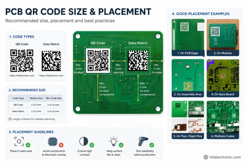
PCB QR Code Size and Placement: Design Rules for Reliable Scanning
Figure 1. PCB QR code size and placement image for PCB...
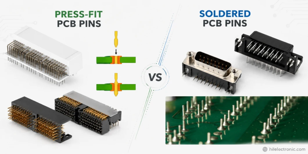
Press-Fit vs Soldered PCB Pins: Header, Connector, and Through-Hole Choices
Figure 1. press-fit vs soldered PCB pins image for PCB...
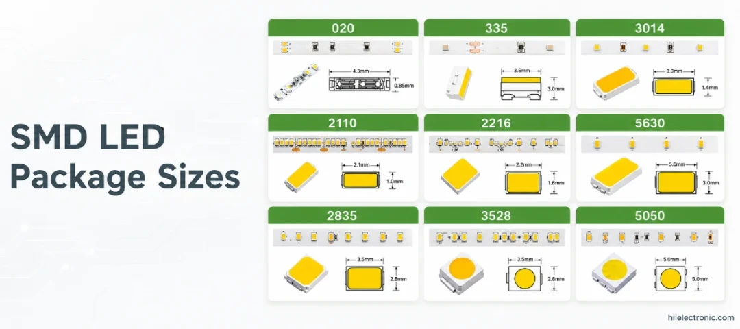
SMD LED Package Sizes: 2835 vs 5050 vs 3528 and PCB Selection
Figure 1. SMD LED package sizes image for PCB...
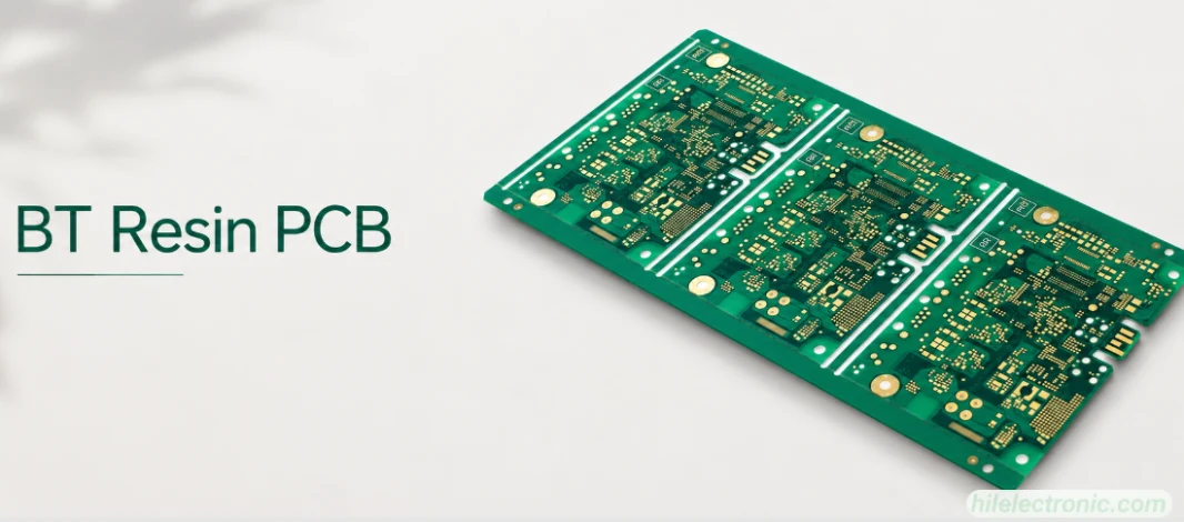
BT Resin PCB: Properties, Uses, and Fabrication Controls
Figure 1. BT resin PCB image for PCB manufacturing...
How to get a quote for PCBs
Let‘s run DFM/DFA analysis for you and get back to you with a report. You can upload your files securely through our website. We require the following information in order to give you a quote:
-
- Gerber, ODB++, or .pcb, spec.
- BOM list if you require assembly
- Quantity
- Turn time
In addition to PCB manufacturing, we offer a comprehensive range of electronic services, including PCB design, PCBA, and turnkey solutions. Whether you need help with prototyping, design verification, component sourcing, or mass production, we provide end-to-end support to ensure your project’s success.
For PCBA services, please provide your BOM (Bill of Materials) and any specific assembly instructions. We also offer DFM/DFA analysis to optimize your designs for manufacturability and assembly, ensuring a smooth production process.