
RFSoC Board PCB Manufacturing and Assembly One-Stop Service
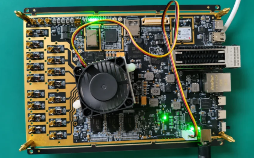
Highleap Electronics supports customer-designed RFSOC board projects with PCB fabrication, component assembly, engineering review, and production support for dense high-speed, RF, memory, optical, and storage hardware.
Reference RFSOC Board Project: 115 × 175 mm, 100G Optical, and NVMe 4.0
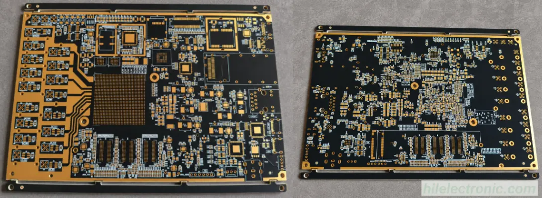
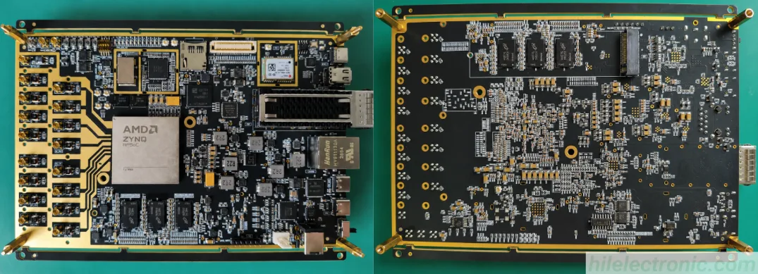
The pictured hardware is a representative high-complexity RFSoC platform with a compact 115 × 175 mm outline, high-speed laminate requirements, a 100G-class optical interface, NVMe 4.0 connectivity, dense BGA devices, memory, power conversion, multiple RF connector channels, and active cooling.
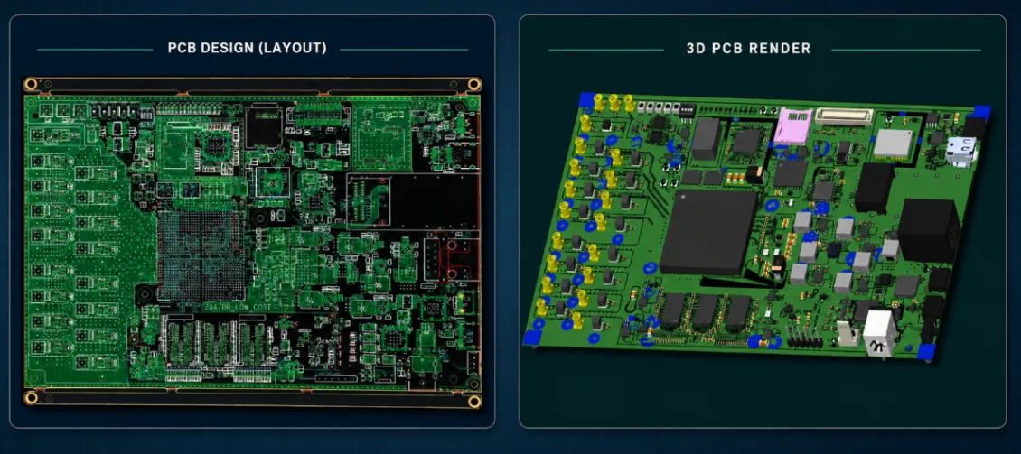
For a PCB factory, this is not simply a “large FPGA board.” It is a mixed-technology manufacturing project in which RF paths, multi-gigabit serial links, memory buses, storage interfaces, power distribution, thermal loading, and mechanical constraints all interact. Manufacturing decisions must therefore follow the customer’s controlled design rather than generic assumptions.
Why RFSOC Board Manufacturing Is More Demanding Than Standard Digital PCB Production
An RFSoC design combines data-converter RF channels and programmable logic with high-speed serial interfaces, memory, storage, clocks, power rails, and mechanical interfaces. The PCB manufacturer must preserve the intent of the design through laminate selection, stack-up construction, imaging, lamination, drilling, plating, etching, solder-mask registration, surface finish, assembly, and inspection.
| Manufacturing area | Why it matters on an RFSOC board | Information required from the customer |
|---|---|---|
| Stack-up and materials | Dielectric thickness, Dk/Df, copper profile, resin system, and glass construction affect impedance and insertion loss. | Approved material family, stack-up, impedance model, loss target, allowable alternatives, and change-control rules. |
| Dense BGA escape | Large RFSoC and memory packages can require fine lines, small vias, via-in-pad, filled/capped structures, or sequential build-up. | BGA pitch, pad design, via type, fill/cap requirement, minimum annular ring, and microsection criteria. |
| RF launch consistency | Connector launches and RF traces are sensitive to geometry, reference planes, pad openings, plating, and local stack-up. | Controlled impedance, connector footprint, launch geometry, RF test coupon, finish, and acceptance method. |
| High-speed serial channels | 100G and PCIe 4.0 links are sensitive to impedance discontinuity, via stubs, roughness, and channel-to-channel variation. | Impedance table, insertion-loss budget, back-drill drawing, pair rules, connector requirements, and coupon plan. |
| Power integrity and thermal load | High-current rails and large BGA packages create copper-balance, thermal-mass, warpage, and reflow challenges. | Copper weights, current requirements, thermal interfaces, heatsink/fixture details, and reflow restrictions. |
High-Speed RFSOC Board PCB Fabrication Priorities
1. Freeze the Material System and Production Stack-Up
“High-speed material” is not a complete fabrication specification. Before tooling, the project should define the laminate and prepreg family, glass styles, resin contents, dielectric thicknesses, copper foil type, copper roughness assumptions, finished copper, total thickness, and approved substitute policy. Highleap’s engineering review converts these requirements into a manufacturable stack-up for customer approval.
2. Translate Impedance and Loss Targets into Factory Controls
Controlled impedance is affected by trace width, spacing, copper thickness, dielectric thickness, etch compensation, solder mask, and local reference-plane geometry. For loss-sensitive links, the customer should also define the relevant frequency range, insertion-loss target, coupon structure, and any roughness or material restrictions. A nominal impedance value alone does not define a complete 100G or PCIe 4.0 channel requirement.
3. Control Via Structures, Stubs, and Back Drilling
Large BGA packages and high-speed connectors often create complex transitions. Blind/buried vias, laser microvias, via-in-pad, conductive or non-conductive fill, cap plating, and back drilling must be clearly identified in the fabrication drawing. Drill depth, residual stub, registration, plating, and inspection criteria should be agreed before production.
4. Manage Registration, Copper Balance, and Flatness
A compact board with dense copper, large BGA fields, RF launch areas, and power circuitry can be sensitive to layer registration and warpage. Balanced copper, suitable panelization, lamination compensation, routing support, and assembly fixtures may be required depending on the final stack-up and component distribution.
Manufacturing Considerations for the 100G Optical Interface
A 100G optical cage or module interface introduces multiple high-speed differential lanes, connector transitions, grounding features, mechanical retention, and thermal constraints. The PCB factory does not “add 100G capability”; it manufactures the customer’s approved channel geometry consistently enough for the design to meet its intended performance.
- Connector footprint and mechanical datum: pad geometry, cage position, mounting holes, keep-outs, and board-edge relationship must match the controlled drawing.
- Differential-pair geometry: line width, spacing, reference plane, neck-down, breakout, and lane-to-lane consistency must be reflected in the stack-up and CAM compensation.
- Via transition control: antipads, ground-via placement, residual stubs, and back-drill requirements should be explicit.
- Insertion-loss management: material, copper roughness, finished copper, path length, and manufacturing tolerance should match the customer’s channel analysis.
- Inspection and verification: impedance coupons, cross-sections, drill verification, electrical test, and any customer-defined signal testing should be included in the quality plan.
NVMe 4.0 / PCIe 4.0 PCB Manufacturing Control
NVMe 4.0 relies on PCIe 4.0 signaling, so the storage channel is sensitive to the same manufacturing variables that affect other multi-gigabit links. Trace geometry and pair spacing must remain consistent from the processor or switch region through vias and connectors to the NVMe device.
During DFM, Highleap reviews the manufacturability of the specified impedance, via structure, back-drill data, connector or M.2 footprint, copper clearances, solder-mask openings, and assembly access. Any proposed change that could affect signal performance should be returned to the customer for approval before fabrication.
RFSOC Board PCB Assembly: BGA, Memory, RF Connectors, and Power Devices
RFSoC PCBA requires more than placing components on a completed bare board. The assembly process must account for large thermal-mass BGAs, memory packages, fine-pitch components, RF connectors, optical cages, storage connectors, power inductors, oscillators, and mechanical hardware.
Assembly engineering priorities
- land-pattern and polarity review against the BOM and assembly drawings;
- stencil aperture design for large BGA, QFN, thermal-pad, and fine-pitch components;
- component moisture sensitivity, baking, storage, and traceability requirements;
- reflow profile development for board thermal mass and component limitations;
- connector seating, coplanarity, mechanical support, and fixture access;
- AOI and X-ray coverage for hidden joints, voiding, bridges, opens, and head-in-pillow risks;
- cleanliness, handling, conformal coating, programming, and functional-test requirements when specified.
Prototype bring-up is especially valuable for an RFSOC board. It allows the customer to verify power sequencing, clocking, programming, thermal behavior, high-speed links, RF paths, peripheral interfaces, and test procedures before repeat production.
How Highleap Electronics Supports a Customer-Designed RFSOC Board
Highleap Electronics operates as a manufacturing partner. We do not market the pictured RFSoC hardware as our own finished product. Our role is to convert the customer’s released design package into controlled PCB and PCBA production.
- RFQ and data review. We review the PCB files, fabrication drawing, stack-up, BOM, assembly data, quantities, delivery target, and test scope.
- PCB DFM and stack-up confirmation. CAM and engineering teams identify manufacturability conflicts, clarify material and via structures, and return a production proposal for approval.
- Component and assembly review. We check package data, BOM status, alternatives, stencil requirements, special handling, fixture needs, and inspection coverage.
- Prototype PCB fabrication and PCBA. The first build follows the approved engineering response and documented process route.
- Inspection and customer-defined testing. Bare-board and assembly inspection are performed according to the agreed quality plan; programming and functional testing follow the customer’s instructions when included.
- Feedback and repeat production. Build findings, approved changes, and test results are incorporated into the controlled manufacturing package for subsequent orders.
What to Send Highleap for an RFSOC Board PCB and PCBA Quotation
For a useful quotation and engineering response, send the most complete package available:
- Gerber, ODB++, or IPC-2581 fabrication data;
- fabrication drawing, drill files, netlist, and controlled stack-up;
- board size, layer count, finished thickness, copper weights, surface finish, and quantity;
- impedance table, insertion-loss requirements, coupon details, and back-drill drawing;
- via-in-pad, fill/cap, microvia, sequential-lamination, and acceptance requirements;
- BOM with manufacturer part numbers, approved alternatives, and sourcing responsibility;
- pick-and-place/centroid file, assembly drawings, polarity notes, and mechanical files;
- programming files, bring-up procedure, test fixture information, and acceptance criteria;
- prototype quantity, forecast volume, target delivery, packaging, and documentation requirements.
RFSOC Board Manufacturing FAQ
Does Highleap Electronics sell the finished RFSOC board shown in the photos?
No. Highleap Electronics is a contract PCB manufacturing and PCB assembly factory. The photos are used to illustrate the type of complex RFSoC hardware we can review for manufacturing. We manufacture customer-designed boards from approved fabrication files, BOMs, assembly drawings, and test requirements; we do not offer the pictured board as a standard catalog product.
What files are needed for an RFSOC board quotation?
Please provide Gerber, ODB++, or IPC-2581 data; fabrication drawing; controlled stack-up; impedance requirements; drill and back-drill information; BOM; centroid file; assembly drawings; programming or test instructions; quantities; and delivery targets. Complete data allows a more accurate DFM review, production route, price, and lead-time estimate.
How are 100G and PCIe 4.0 signal-integrity requirements protected during PCB production?
The approved stack-up, trace geometry, dielectric construction, copper characteristics, via transitions, back-drill requirements, and impedance coupons must be translated into controlled fabrication instructions. Any material or geometry change should be reviewed and approved before production because system performance depends on both the design and the manufactured result.
Can Highleap provide both bare PCB fabrication and PCBA for an RFSoC design?
Yes. Highleap Electronics supports integrated PCB fabrication and PCB assembly so the customer can manage the project through one manufacturing partner. The exact scope can include material review, DFM, bare-board fabrication, component sourcing support, SMT/THT assembly, inspection, programming, and customer-defined functional testing.
Can prototype builds be completed before volume production?
Yes. A controlled prototype or engineering build is recommended for dense RFSoC hardware because it allows the customer and factory to verify manufacturability, assembly yield, programming, bring-up, thermal behavior, and test coverage before the production package is frozen.
The RFSoC board images on this page are used only to illustrate manufacturing complexity and are not an offer to sell the pictured finished board. Product ownership, design rights, and technical specifications remain with the respective design owner.

Recommended Posts

TMM4 Filter PCB Manufacturing
TMM4 filter PCB manufacturing is controlled by the...

TMM3 PCB Manufacturing for RF Modules
TMM3 PCB manufacturing is most useful where the RF module...

TMM6 PCB Fabrication
TMM6 fabrication is the process-control page for a mid-Dk...

TMM10 PCB Manufacturing for Compact RF Designs
Table of contentsHow TMM10 Shrinks RF StructuresTMM10 vs...
How to get a quote for PCBs
Let’s run DFM/DFA analysis for you and get back to you with a report. You can upload your files securely through our website. We require the following information in order to give you a quote:
-
- Gerber, ODB++, or .pcb, spec.
- BOM list if you require assembly
- Quantity
- Turn time
For PCBA services, please provide your BOM (Bill of Materials) and any specific assembly instructions. We also offer DFM/DFA analysis to optimize your designs for manufacturability and assembly, ensuring a smooth production process.