
High-Speed RF DAC PCB Assembly
Highleap Electronics supports high-speed RF DAC, FPGA and mixed-signal electronics with PCB fabrication, component sourcing, SMT/THT assembly, BGA inspection and project-defined testing — from prototype builds through repeatable production.
For high-speed converter PCBAs, manufacturing quality depends on the bare-board stack-up, controlled impedance, material selection, via structures, component packages, assembly process and inspection strategy working together.
Why high-speed RF DAC PCB assembly needs tighter manufacturing control
RF DAC boards sit at the intersection of high-speed digital, precision clocking, analog/RF signal paths and complex power delivery. The challenge for a PCB manufacturer and assembler is not simply to build a dense board — it is to reproduce the released design without introducing manufacturing variation that can undermine signal integrity, assembly yield or test repeatability.
Devices in this class can use very fast serial interfaces such as JESD204B/JESD204C. For example, TI's DAC39RF10 is a 16-bit, two-channel RF DAC with up to 20.48 GSPS conversion capability and JESD204B/C interfaces. That technology context explains why PCB stack-up, impedance, via transitions, BGA assembly and clock/power integrity matter so much in this category.
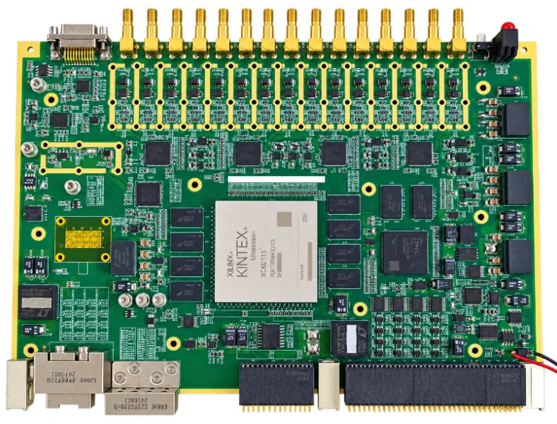
Build the bare PCB around the electrical requirements of the RF DAC design
For a high-speed RF DAC PCB, fabrication decisions can directly affect the transmission structures created by the layout. Highleap's role is to manufacture the released board to the specified stack-up, controlled-impedance requirements, material system and mechanical tolerances while identifying manufacturability conflicts before production.
Stack-up & controlled impedance
Trace geometry, copper thickness, dielectric thickness and dielectric properties work together. If the design depends on a specific impedance structure, stack-up changes should be reviewed rather than treated as routine substitutions.
High-speed via structures
Via-in-pad, filled/capped vias, blind/buried vias, back-drilling or other stub-control methods may be required by the design. The correct structure depends on routing density, board thickness and the electrical channel requirements.
RF / high-speed materials
Material should follow the actual loss budget, frequency, route length, thermal environment and cost target. Highleap manufactures conventional multilayer boards as well as high-speed and RF/microwave PCB constructions using customer-specified materials.
Fabrication DFM
Drill-to-copper clearance, annular ring, fine lines, copper balance, registration, panelization and special processes should be reviewed before the board is released to production.
RF DAC and FPGA PCBAs need assembly controls for dense packages and mixed thermal mass
High-speed converter boards often combine large BGAs, QFNs, memory, clock devices, small passives, power modules and large board-level connectors. A stable PCB assembly process has to manage those package differences through stencil design, solder-paste printing, component placement, reflow and secondary assembly.
FPGA / BGA assembly
Large BGAs create hidden solder joints and can be sensitive to package warpage, paste volume, thermal profile and pad/via construction. Assembly review should begin before the first larger NPI build.
Fine-pitch RF components
QFN, LGA and other fine-pitch packages require accurate footprints, controlled paste deposition and placement consistency. Hidden or partially hidden joints may require X-ray inspection.
Power modules & thermal mass
High-current power sections can create very different heating behavior from small signal components. Reflow profiling and any secondary soldering process should reflect the actual component mix.
Connectors & mixed technology
Large connectors may require through-hole, selective soldering, press-fit or other project-specific processes. Mechanical alignment and board support should be included in assembly planning.
One workflow for PCB fabrication and PCB assembly
Highleap's published PCB assembly services include PCB manufacturing coordination, component sourcing, SMT, through-hole assembly, AOI, X-ray inspection, IC programming and functional testing. Keeping fabrication and assembly in one workflow reduces handoffs between the bare-board and PCBA stages.
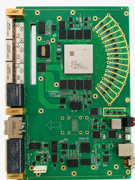
The BOM is part of the manufacturing risk for FPGA and RF DAC PCBAs
High-value converters, FPGAs, memories, oscillators, power modules and specialized connectors can affect both project cost and production timing. Component sourcing therefore needs to be reviewed before a prototype turns into a pilot or production order.
Use exact manufacturer part numbers
Generic descriptions are not enough for controlled purchasing. The BOM should identify approved manufacturer part numbers for devices where electrical performance, package or firmware compatibility matters.
Alternates require approval
A substitute should not be accepted simply because the footprint fits. Electrical characteristics, temperature range, timing, package details and qualification requirements can all matter.
Review lifecycle and lead time
Long-lead, allocated or end-of-life components can delay a pilot or production build. Early sourcing review helps the project team make decisions before larger material commitments.
Turnkey or customer-supplied parts
Projects can be structured around turnkey sourcing, consigned components or a mixed model depending on the customer's supply-chain requirements.
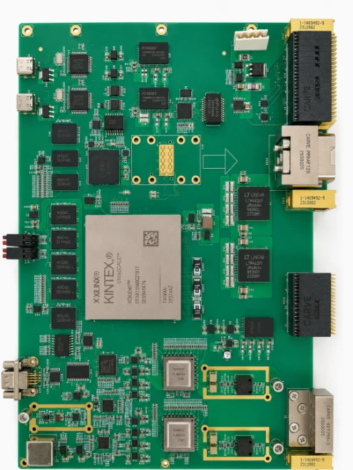
AOI, X-ray and functional testing verify different parts of PCBA quality
No single inspection method can prove everything about a high-speed RF DAC assembly. The inspection and test plan should be matched to the component package mix, design-for-test access and customer acceptance requirements.
| Method | What it helps verify | Key limitation |
|---|---|---|
| AOI | Visible component presence, orientation, placement and solder-related conditions. | Cannot directly inspect solder joints hidden beneath BGAs and some bottom-terminated packages. |
| X-ray | Hidden solder-joint structures under BGA, QFN and similar packages. | Inspection criteria still need to match package type and customer requirements. |
| Electrical test | Selected electrical conditions, opens/shorts or other checks depending on test access and method. | Coverage depends on design-for-test and the test program. |
| Functional test | Project-defined power-up, interfaces, firmware and functional behavior. | Requires the expected behavior, test method and pass/fail limits to be defined. |
Highleap's published PCB assembly capabilities include AOI, X-ray inspection and functional testing. For functional testing, the scope is built around the customer's product requirements, firmware, interfaces and acceptance criteria.
A successful prototype is the start of the manufacturing process, not the end
A board can function in the lab and still need manufacturing work before it is ready for repeatable production. High-speed RF DAC PCBAs benefit from a staged approach that finds fabrication, sourcing, assembly and testing issues before larger quantities are committed.
A PCB manufacturer and PCB assembly partner for high-speed RF DAC projects
PCB fabrication under the same manufacturing partner
Highleap manufactures multilayer, high-speed, RF/microwave and other complex PCB technologies from prototype through production.
Component sourcing + PCBA
Turnkey support can combine bare-board fabrication, component procurement, SMT/THT assembly and final inspection in one workflow.
Inspection for dense packages
AOI and X-ray support inspection of visible assembly conditions and hidden solder-joint structures where appropriate.
Project-defined testing
Functional testing and IC programming can be incorporated when the customer provides or defines the relevant requirements.
You do not need to be a PCB engineer to start a quotation
Many purchasing teams receive technical files from engineering without knowing which file is a Gerber, BOM or pick-and-place file. That should not stop the first conversation. Start with the commercial requirement and send the project information you already have.
Tell us what you need
Choose bare PCB, PCB assembly, turnkey PCBA, or tell us that you are not sure yet.
Tell us quantity and schedule
Prototype quantity, pilot quantity or production demand gives the manufacturing team the commercial context.
Send whatever files you have
Upload the engineering folder, BOM, drawings or previous supplier package as-is. Highleap can identify what additional information is needed for an accurate manufacturing review.
Helpful information — if you already know it
Before production, complete PCB and assembly data will still be required. The difference is that Highleap's engineering team can tell you what is missing after the initial review instead of expecting purchasing to identify every technical document in advance.
High-Speed RF DAC PCB Assembly FAQ
What is high-speed RF DAC PCB assembly?
It is the manufacturing and assembly of PCBAs that combine high-speed digital processing, RF or wideband DACs, precision clocking, analog/RF signal paths and power circuitry. These boards often require controlled-impedance PCB fabrication, dense SMT/BGA assembly and inspection methods matched to hidden solder joints.
Does every RF DAC PCB require Rogers or another RF laminate?
No. Material should be selected according to the design's frequency, insertion-loss budget, route length, impedance requirements, thermal environment and cost target. Some designs use high-performance FR-4; others require lower-loss or hybrid constructions.
Can Highleap provide both PCB fabrication and PCB assembly?
Yes. Highleap's published services include PCB fabrication, component sourcing, SMT and through-hole assembly, inspection, testing and turnkey PCB assembly.
How are FPGA and BGA solder joints inspected?
AOI is useful for visible assembly conditions, while X-ray inspection can support evaluation of hidden solder-joint structures beneath BGA and similar packages. The inspection scope should be matched to the package and project requirements.
What if purchasing does not know which PCB files are required?
Start by sending the files you already have together with the required service, quantity and schedule. Highleap can review the package and identify additional information needed before an accurate quotation or production release.
Build your high-speed RF DAC PCB and PCBA with one manufacturing partner.
From high-speed and RF PCB fabrication through component sourcing, SMT/BGA assembly, AOI, X-ray and project-defined functional testing, Highleap supports the transition from prototype builds to repeatable production.
Final stack-up, material, impedance, assembly, inspection and test requirements should be defined for the specific customer design before production.
Recommended Posts
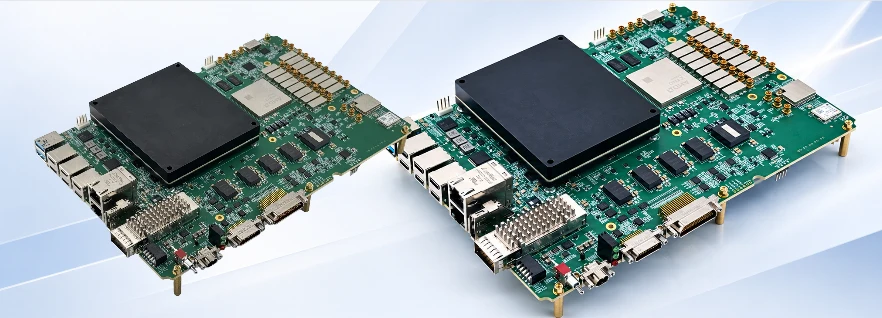
High-Speed RFSoC PCB Manufacturing and Assembly: Key Engineering Considerations
How to get a quote for PCBs Let's run DFM/DFA analysis for...

1206 PCB Assembly Services for Prototypes & Production
src="https://hilelectronic.com/wp-content/uploads/2026/08/PC...

Kitted PCBA Services for Customer-Supplied Components
Kitted PCBA is a manufacturing model in which the customer...

Build to Print PCB Assembly Services
src="https://hilelectronic.com/wp-content/uploads/2026/08/PC...
How to get a quote for PCBs
Let’s run DFM/DFA analysis for you and get back to you with a report. You can upload your files securely through our website. We require the following information in order to give you a quote:
-
- Gerber, ODB++, or .pcb, spec.
- BOM list if you require assembly
- Quantity
- Turn time
For PCBA services, please provide your BOM (Bill of Materials) and any specific assembly instructions. We also offer DFM/DFA analysis to optimize your designs for manufacturability and assembly, ensuring a smooth production process.