
High Speed PCB Manufacturing: Advanced Capabilities of Highleap Electronics

Introduction
High Speed PCB Manufacturing has become a critical factor as modern electronics push the limits of data transmission in AI servers, 5G infrastructure, and high-performance networking systems. These advanced applications require precise signal integrity, tight impedance control, and manufacturing processes capable of supporting multi-gigabit data rates without reliability issues.
Choosing the right high speed PCB manufacturer directly impacts whether your design achieves the expected performance and stability. Unlike standard PCB production, high speed PCB fabrication demands specialized expertise, advanced equipment, and proven processes that only experienced manufacturers can deliver.
At Highleap Electronics, we combine advanced high speed PCB manufacturing capabilities with engineering expertise to help customers bring complex designs to reliable, production-ready solutions.
What Makes High Speed PCB Manufacturing Different?
High Speed PCB manufacturing is fundamentally different from conventional PCB production because signal integrity becomes critical at high frequencies and fast data rates. Every design decision—from materials to layer stack-up—must be optimized to prevent signal loss and distortion.
Signal Integrity Requirements
High-speed digital signals are extremely sensitive to distortion that can compromise system performance. Controlled impedance is essential, often requiring tolerances of ±5% or tighter, compared to ±10% for standard PCBs. Differential pair routing demands precise trace spacing and consistent dielectric properties across the entire board to maintain signal quality.
Advanced Manufacturing Processes
High density interconnect (HDI) technology enables the fine geometries required for today’s high speed applications. Laser-drilled microvias as small as 0.1mm support compact routing, while sequential lamination allows buried and blind vias that shorten signal paths and reduce parasitic effects.
Stringent Testing Standards
High speed PCBs require more than standard continuity checks. Time domain reflectometry (TDR) validates impedance along the entire signal path. Flying probe testing ensures electrical performance meets specifications before assembly, and automated optical inspection (AOI) verifies geometric accuracy of critical features.
These specialized requirements make high speed PCB manufacturing a field where experience and advanced capabilities matter. At Highleap Electronics, we apply proven processes and rigorous testing to ensure every board delivers consistent high-speed performance.
Highleap’s High Speed PCB Manufacturing Capabilities
At Highleap Electronics, our high speed PCB manufacturing capabilities are built to support demanding digital applications in AI servers, 5G infrastructure, networking systems, and advanced industrial electronics. Every process is designed to deliver reliable performance, precise impedance control, and fast turnaround times.
| Specification | Capability |
|---|---|
| Layer Count | Up to 32 layers with sequential lamination |
| Minimum Line/Space | 2.5/2.5 mil (63.5μm/63.5μm) |
| Via Technology | Laser drilled microvias, 0.1mm minimum |
| Impedance Control | ±3% tolerance with full documentation |
| HDI Capabilities | 1+N+1 to 3+N+3 constructions |
| Aspect Ratio | Up to 12:1 for through holes |
| Registration Accuracy | ±0.03mm (1.2 mil) |
| Surface Finish Options | ENIG, OSP, Immersion Silver, Hard Gold |
Production Flexibility and Capacity
We provide full flexibility to support both rapid prototyping and large-scale production. Quick-turn services can deliver fully functional high speed PCB prototypes within 3–5 business days, helping customers accelerate their development cycles. For volume production, our optimized processes ensure consistent quality across thousands of boards, without compromising lead time.
Specialized Equipment Investment
Our facilities are equipped with advanced systems dedicated to high speed PCB production. This includes multiple laser drilling machines for 0.1mm microvias, automated optical inspection (AOI) systems with sub-micron resolution, and precision impedance testing equipment calibrated to aerospace standards. These investments allow us to maintain tight process control and deliver boards that meet the most stringent requirements.
By combining scalable production capacity with advanced equipment, Highleap offers a manufacturing platform that ensures both performance and reliability for every high speed PCB project.
Advanced Materials for High Speed PCB Manufacturing
Material selection plays a decisive role in high speed PCB manufacturing, since dielectric stability and low-loss properties directly affect signal integrity at elevated frequencies. The right choice of high speed PCB materials ensures consistent performance, reliability, and compliance with the most demanding industry standards.
Low-Loss Dielectric Materials
We stock a wide range of specialized low-loss materials designed for high-speed applications. Rogers RO4350B provides excellent electrical properties while remaining compatible with standard PCB processes. Isola IS620 delivers ultra-low loss characteristics for advanced designs, while the Panasonic Megtron series ensures stable performance across wide frequency ranges. This broad material selection allows us to meet diverse application needs from 5G to AI computing.
Copper Foil Considerations
For high-frequency designs, copper surface profile is a key factor. Low-profile copper foils reduce insertion loss and improve overall signal quality. Depending on your application, we offer standard ED (electrodeposited) and VLP (very low profile) copper options, ensuring the best balance of cost and performance for each project.
Material Qualification and Traceability
Every material used in our high speed PCB production undergoes rigorous incoming inspection and qualification testing. Full lot traceability guarantees consistent electrical properties, while material certifications provide complete documentation for customer assurance. This strict quality process minimizes risks and gives customers confidence in long-term reliability.
By combining extensive material options with strict qualification and traceability, Highleap Electronics ensures that every high speed PCB we manufacture is optimized for performance, reliability, and consistency.

Quality Assurance and Testing
Our comprehensive quality assurance processes ensure that every board produced through high speed PCB manufacturing meets exact specifications and delivers consistent, reliable performance in the field.
Impedance Testing and Control
Impedance stability is the most critical factor in high speed PCB quality. Using calibrated TDR equipment, we measure impedance at multiple points along critical signal traces to guarantee accuracy. Statistical process control techniques track variations in real time, enabling continuous improvement and process stability.
Special attention is given to differential pair impedance matching. We achieve ±1Ω precision within the same differential signal group, ensuring superior noise rejection and minimal skew—key to maintaining signal integrity at multi-gigabit speeds.
Advanced Inspection Techniques
We employ advanced inspection systems to detect and prevent defects early in production. Automated optical inspection (AOI) with sub-micron resolution identifies dimensional or registration errors, while X-ray inspection reveals hidden defects in vias. Cross-sectional analysis verifies dielectric and copper thickness, as well as via quality, providing additional assurance of long-term reliability.
Certification Standards Compliance
All of our high speed PCB manufacturing processes comply with globally recognized standards, including IPC-6012 Class 3 for high-reliability electronics, IPC-A-600 acceptability standards, and ISO 9001:2015 quality management. We are also IATF 16949 certified, ensuring compliance with automotive industry requirements.
Through strict testing, inspection, and certification, Highleap Electronics delivers high speed PCBs that consistently perform under the most demanding conditions, giving customers confidence in both product quality and long-term reliability.
Why Choose Highleap for High Speed PCB Manufacturing
Choosing the right partner for high speed PCB manufacturing is critical to ensuring performance, reliability, and on-time delivery. Highleap Electronics stands out by combining technical expertise with scalable production capacity and responsive customer support.
Our Advantages
- Advanced Manufacturing: Up to 32-layer HDI stack-ups, laser-drilled microvias, and precise impedance control (±3%).
- One-Stop Service: PCB fabrication, PCB assembly, and component sourcing integrated into a single streamlined process.
- Engineering Expertise: DFM analysis, stack-up recommendations, and pre-production design reviews for signal integrity optimization.
- Quality Assurance: Rigorous testing, IPC Class 3 standards, ISO 9001, and IATF 16949 certification for reliability in demanding industries.
- Global Logistics: Multiple facilities and established supply chains ensure flexible capacity and fast worldwide delivery.
Partner with Highleap Electronics
Looking for a trusted partner in high speed PCB manufacturing? Highleap Electronics delivers proven expertise, reliable quality, and fast turnaround for your most challenging projects. Contact our team today to discuss your requirements and receive a customized quotation.

Recommended Posts
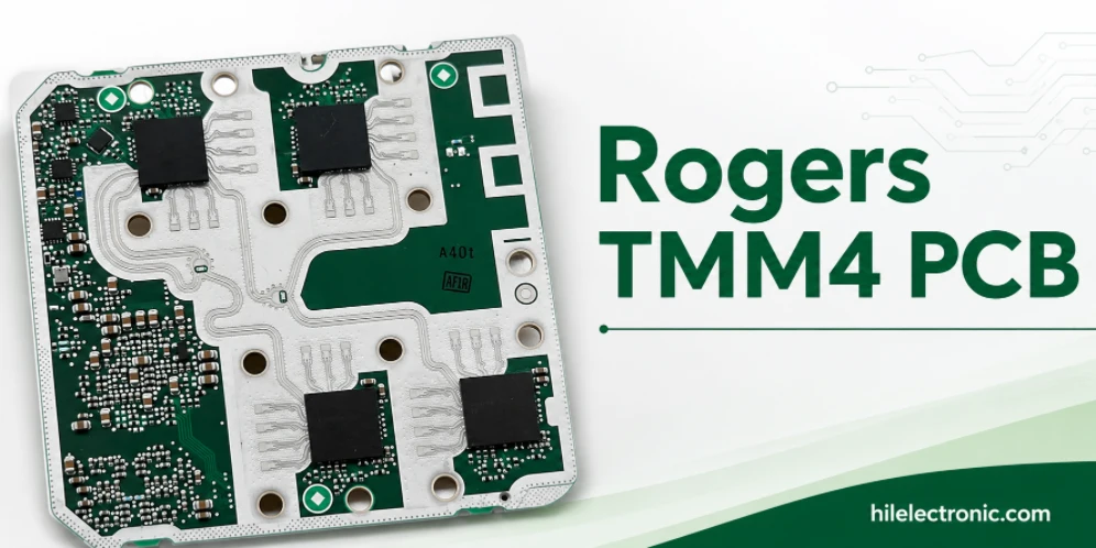
Rogers TMM4 PCB Manufacturer for Compact Microwave Filters
TMM4 is most useful when a microwave circuit must become...
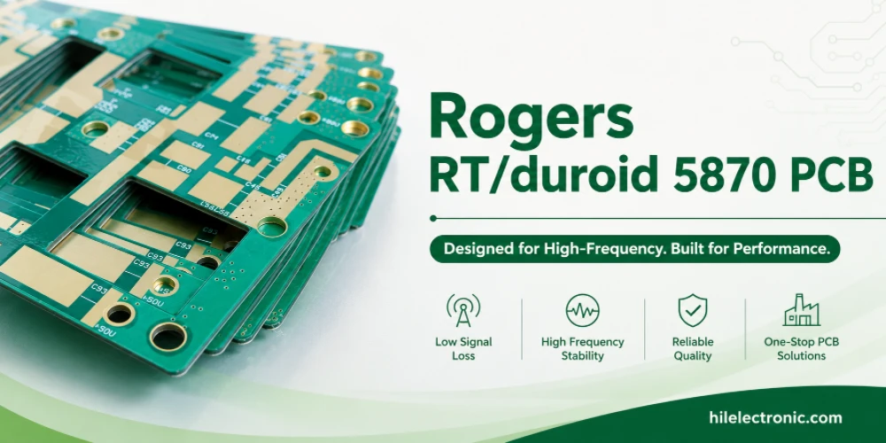
RT/duroid 5870 PCB Manufacturer for Low-Loss PTFE RF Circuits
RT/duroid 5870 is chosen when the RF path needs low loss,...
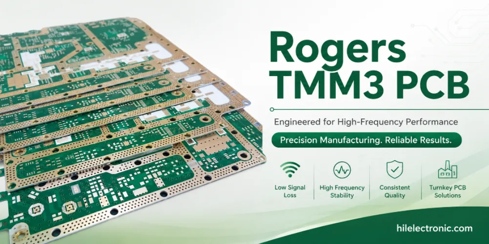
Rogers TMM3 PCB Manufacturer for Mechanical RF Modules
TMM3 is selected when an RF circuit must behave as part of...
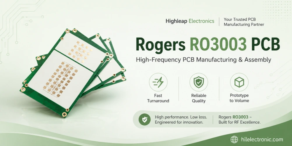
Rogers RO3003 PCB Manufacturer for Automotive Radar and mmWave Modules
A 77 GHz radar board is purchased as a working sensor...
How to get a quote for PCBs
Let‘s run DFM/DFA analysis for you and get back to you with a report. You can upload your files securely through our website. We require the following information in order to give you a quote:
-
- Gerber, ODB++, or .pcb, spec.
- BOM list if you require assembly
- Quantity
- Turn time
In addition to PCB manufacturing, we offer a comprehensive range of electronic services, including PCB design, PCBA, and turnkey solutions. Whether you need help with prototyping, design verification, component sourcing, or mass production, we provide end-to-end support to ensure your project’s success.
For PCBA services, please provide your BOM (Bill of Materials) and any specific assembly instructions. We also offer DFM/DFA analysis to optimize your designs for manufacturability and assembly, ensuring a smooth production process.