
PCB Backdrilling | Controlled Depth Drilling | Advanced PCB Manufacturing

What is PCB Backdrilling?
PCB backdrilling, also known as controlled-depth drilling, involves the removal of stubs in multi-layer PCBs to create plated through-holes. The purpose of backdrilling is to facilitate the flow of signals between different layers of the circuit board without interference from unnecessary stubs.
For a clearer explanation of the backdrilling process, let’s consider an example. Imagine a 12-layer PCB with plated through-holes connecting the first and twelfth layers. The goal is to connect only the first layer to the ninth layer while keeping the tenth to twelfth layers unconnected. However, the unconnected layers create “stubs” that can potentially disrupt signal paths, leading to signal integrity issues. Backdrilling involves drilling out these short stubs from the backside of the PCB to improve signal transmission.
So, when is backdrilling used? It is generally recommended to consider this technique when signals on the PCB board operate at rates of ≥1 Gbps. However, designing high-speed interconnects is a complex system engineering task that should also take into account factors like the chip’s driving capabilities and the length of the interconnect links. Therefore, performing system-level interconnect simulations is the most reliable way to determine the need for backdrilling.
Advantages and Disadvantages of Backdrilling
Advantages of PCB Backdrilling
- Reduces Signal Attenuation: Backdrilling helps reduce signal attenuation, ensuring stronger and more reliable signals. Additionally, this technique minimizes the impact of stubs on impedance matching, which in turn reduces EMI/EMC radiation.
- Prevents Signal Distortion: Backdrilling is an effective method for preventing signal distortion issues. It is well-known that via stubs can introduce deterministic jitter, possibly caused by signal crosstalk, electromagnetic interference, and noise. By eliminating these stubs, backdrilling helps eliminate sources of deterministic jitter, improving signal quality and preventing signal distortion.
- Minimizes Crosstalk Between Vias: Backdrilling holes contribute to minimizing crosstalk between plated through-holes.
- Reduces Deterministic Jitter: Implementing backdrilling can reduce deterministic jitter in signals, which can lead to an overall decrease in the bit error rate (BER) of the signals.
- Decreases Excitation of Resonance Modes: Backdrilling helps reduce the excitation of resonance modes.
- Minimizes the Use of Buried and Blind Vias: It simplifies PCB manufacturing by reducing the need for buried and blind vias.
- Minimal Impact on Design and Layout: Backdrilling has minimal impact on the overall design and layout.
- Expands Channel Bandwidth: It allows for the expansion of channel bandwidth.
- Lower Cost Compared to Sequential Lamination: Backdrilling can be more cost-effective compared to sequential lamination.
Disadvantages of PCB Backdrilling
Frequency Limitation: Backdrilling is suitable for signal frequencies in the range of 1 GHz to 3 GHz and may not be viable for high-frequency boards with blind vias. Special techniques are needed to prevent any lateral traces and planes on the backside of the board from being damaged during backdrilling.
PCB Backdrilling Process
- Drilling Holes in the PCB: Holes are drilled in the PCB to create plated through-holes connecting multiple layers of the circuit board.
- Sealing Positioning Holes with Dry Film: Positioning holes are sealed with dry film before electroplating the holes to create conductive pathways.
- Copper Plating of Holes: Copper is plated onto the holes to create the conductive paths.
- Outer Layer Graphics Creation: After creating the outer layer graphics, graphic electroplating is performed on the PCB. Proper treatment of the sealed positioning holes is crucial before this process.
- Backdrilling Execution: During the initial drilling process, the positioning holes used for alignment in the backdrilling process are used, and the plated holes from this process are backdrilled.
- Cleaning the PCB: After backdrilling, it is necessary to clean the PCB to remove any residual drill debris.
- Inspection of the PCB: The PCB is inspected to verify the accuracy of the backdrilling process and to ensure enhanced signal integrity.
PCB Backdrilling Design Tips
To ensure proper backdrilling, it is essential to provide the PCB manufacturer with separate output files containing the backdrilling layers and detailed specifications of which layers require corresponding backdrilling. The diameter of backdrilled holes should be at least 0.2mm larger than the diameter of the first hole, with a distance of 0.35mm for the first drill and 0.2mm for the backdrill from the traces. During PCB layer stack-up design, consideration should be given to the dielectric thickness to avoid drilling into traces that should not be drilled into. If specific layers require drilling (e.g., “large” layers), the dielectric thickness between non-drilled and adjacent layers should be at least 0.2mm.
Additionally, optimizing the backdrilling process involves minimizing the number of blind and buried vias and avoiding them in less critical areas. Placing vias in less critical areas and maintaining minimum distances between backdrill holes and signal traces also helps prevent signal reflections and other issues. Keeping backdrilled hole diameters small is crucial to avoid damaging lateral traces and planes on the backside of the board. Furthermore, considering backdrilling during the initial design phase helps ensure necessary steps are taken to optimize signal integrity and prevent issues during the manufacturing process.
Challenges in the Backdrilling Process
Control of Backdrilling Depth: Controlling the depth of backdrilling is crucial for precise machining of blind vias. The backdrilling depth tolerance is primarily influenced by the accuracy of the backdrilling equipment and the tolerance of dielectric thickness. However, external factors such as drill bit resistance, drill tip angle, contact effects between the cover plate and the measuring unit, and board flexing can also affect backdrilling precision. During the production process, selecting the right drilling material and method is crucial for achieving optimal results and controlling backdrilling accuracy. By carefully controlling the depth of backdrilling, design engineers can ensure high-quality signal transmission and prevent signal integrity issues.
Control of Backdrilling Precision: Precise control of backdrilling is essential for quality control of the PCB in subsequent processes. Backdrilling involves secondary drilling based on the diameter of the primary hole, and the precision of this secondary drilling is critical. Several factors, including board expansion and contraction, equipment accuracy, and drilling methods, can influence the precision of overlapping secondary drills. Therefore, it is important to ensure accurate control of the backdrilling process to minimize errors and ensure optimal signal transmission and integrity.

Application of PCB Backdrilling
PCB backdrilling is commonly applied in multilayer designs where unused via stubs can degrade signal integrity at high data rates. By removing the unused plated-through hole section, backdrilling reduces reflections, jitter risk, and insertion loss on critical interconnects—especially when interfaces operate around gigabit speeds and above. For design context, many teams evaluate backdrilling together with high-speed PCB layout and routing practices and confirm requirements through stackup and channel constraints.
- Telecommunications and networking infrastructure: Base stations, optical transport, routers, and switches depend on clean high-speed channels. Backdrilling is often used on backplane and line-card designs to reduce stub-related discontinuities and improve margin on critical links.
- Data servers and data centers: Compute platforms and high-bandwidth switching systems benefit from reduced via-stub resonance and cleaner return paths. Backdrilling helps support stable performance as lane speeds increase across dense multilayer boards.
- High-performance computing and test equipment: Supercomputing nodes, high-speed instrumentation, and lab measurement platforms require repeatable channel behavior. Backdrilling can improve link consistency by minimizing discontinuities caused by unused via barrel length.
- Consumer electronics with high data throughput: Flagship smartphones, tablets, and high-resolution displays may use backdrilling in compact multilayer PCBs to support demanding video and data interfaces without excessive signal distortion.
- Medical, aerospace, and defense electronics: Systems such as imaging, avionics, radar, and satellite communications often prioritize deterministic signal performance. Backdrilling is used where multilayer routing density and reliability requirements make stub control important.
- Automotive electronics: Advanced driver assistance, domain controllers, and vehicle communications increasingly use high-speed interfaces. Backdrilling can be part of the strategy to limit reflections and preserve signal margin in dense automotive multilayer builds.
- Industrial automation: Motion control, machine vision, and industrial networking platforms may adopt backdrilling to maintain signal quality across dense interconnects in electrically noisy environments.
In practice, backdrilling is usually specified as part of an overall channel strategy that includes controlled impedance planning and via modeling. Where stub resonance and via transitions are a primary concern, engineers often reference via behavior in high-frequency environments (including stub resonance) alongside backdrilling decisions; see RF PCB via design considerations.
Unlock the full potential of your electronic designs with Highleap Electronic’s cutting-edge PCB backdrilling and HDI PCB manufacturing solutions. Whether you’re building high-speed telecommunications equipment, advanced medical devices, or automotive systems, our expertise ensures unparalleled signal integrity and performance. By eliminating unwanted stubs, reducing crosstalk, and optimizing channel bandwidth, our backdrilling process delivers superior signal quality for even the most demanding applications. With precision engineering, advanced materials, and cost-efficient production strategies, Highleap Electronic is your trusted partner for high-performance, reliable, and innovative PCBs. Elevate your products today—contact us for a custom consultation and see the difference precision makes!
FAQs:
1. What is the primary purpose of PCB backdrilling?
PCB backdrilling is used to remove unnecessary via stubs in multi-layer PCBs to improve signal integrity, reduce crosstalk, and enhance the overall performance of high-speed electronic systems.
2. How does PCB backdrilling impact signal integrity in high-frequency designs?
Backdrilling eliminates stubs that cause signal reflections, crosstalk, and jitter, resulting in clearer, more reliable signal transmission at frequencies typically above 1 GHz.
3. What are the challenges in controlling backdrilling depth?
Controlling backdrilling depth is influenced by factors like drill bit resistance, equipment accuracy, and dielectric thickness. Precise depth control is critical to avoid damaging non-target layers or traces.
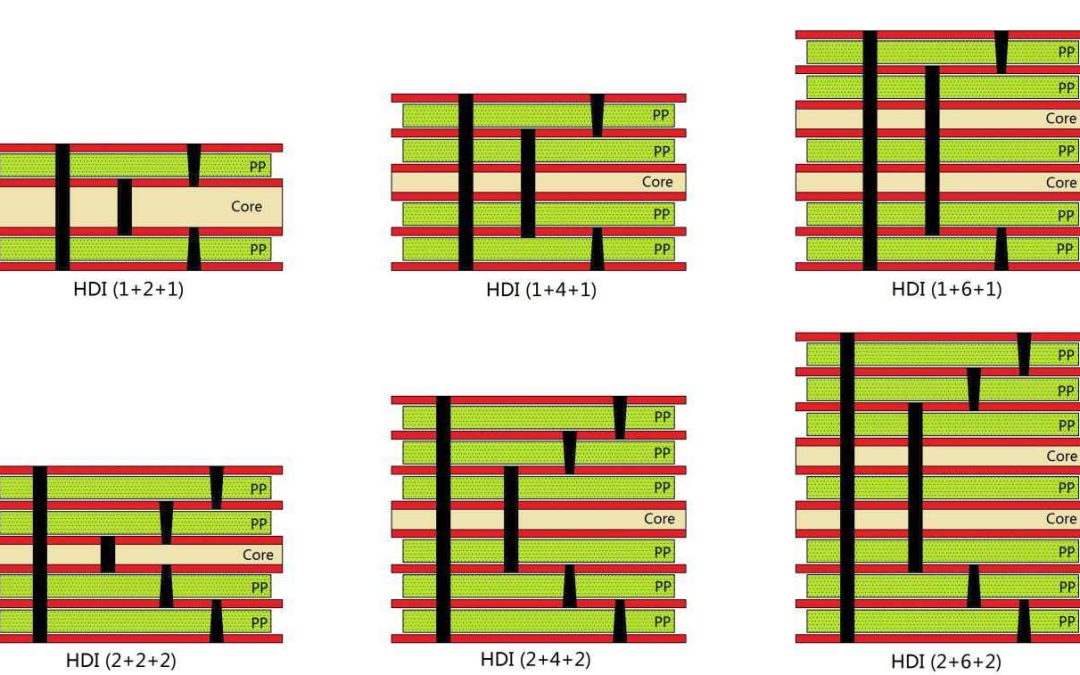
4. Is backdrilling suitable for HDI PCB designs with blind and buried vias?
Backdrilling is less commonly used for HDI PCBs with blind and buried vias. However, when needed, special techniques are employed to maintain the integrity of high-density interconnections.
5. How do manufacturers ensure precision during the backdrilling process?
Manufacturers use advanced equipment, tight tolerances, and robust quality control measures, including automated optical inspection and X-ray inspection, to ensure backdrilling precision.
6. What industries benefit the most from PCB backdrilling?
Industries such as telecommunications, data centers, aerospace, medical devices, and automotive electronics benefit greatly from backdrilling due to their reliance on high-speed and high-frequency signal integrity.
Get a Free PCB & PCBA Quote

Recommended Posts

Comprehensive Guide to Plated Through-Hole (PTH) Technology in PCB Manufacturing
[pac_divi_table_of_contents title="On this article"...

Mastering Staggered and Stacked Vias: Advanced PCB Design Techniques for High-Performance Electronics
An important part of modern PCB design is PCB drilling -...

High Density Interconnect PCB Guide | Highleap Electronics
[pac_divi_table_of_contents...
HDI Layout Best Practices: Key Design Tips for HDI Circuit Boards
HDI stack diagram in HDI circuit board factoryIntroduction...
How to get a quote for PCBs
Let us run DFM/DFA analysis for you and get back to you with a report.
You can upload your files securely through our website.
We require the following information in order to give you a quote:
-
- Gerber, ODB++, or .pcb, spec.
- BOM list if you require assembly
- Quantity
- Turn time
In addition to PCB manufacturing, we offer a comprehensive range of electronic services, including PCB design, PCBA (Printed Circuit Board Assembly), and turnkey solutions. Whether you need help with prototyping, design verification, component sourcing, or mass production, we provide end-to-end support to ensure your project’s success. For PCBA services, please provide your BOM (Bill of Materials) and any specific assembly instructions. We also offer DFM/DFA analysis to optimize your designs for manufacturability and assembly, ensuring a smooth production process.