
RF PCB Impedance Control: Design Guide & Calculations

Impedance control for RF PCB designs determines whether high-frequency circuits deliver optimal performance or suffer from signal reflections and power loss that compromise system functionality. Modern wireless devices and communication equipment demand precise impedance matching throughout the signal path to maintain signal integrity above 1 GHz. This guide covers transmission line fundamentals, calculation methods, material selection, and design rules for achieving consistent 50Ω impedance in production.
Why Impedance Control for RF PCB Design Is Critical
Signal Integrity Impact
Uncontrolled impedance in RF PCB traces creates reflections that degrade performance through insertion loss, phase errors, and harmonic distortion. The reflection coefficient Γ = (ZL – Z₀)/(ZL + Z₀) quantifies reflected energy when impedances mismatch. For example, connecting a 50Ω source to a 75Ω load produces Γ = 0.2, reflecting 4% of incident power and creating 1.5:1 VSWR.
System-Level Effects
Impedance discontinuities affect antenna networks, filter responses, and amplifier stability in ways that compound across RF chains. A 10% variation acceptable at 100 MHz causes significant phase errors at 5 GHz where wavelengths are shorter. Precise impedance control for RF PCB manufacturing ensures predictable S-parameters and first-pass design success.

Microstrip
PCB Transmission Line Types
1. Microstrip — Advantages and Limitations
Microstrip routes RF signals on outer layers above a ground plane, balancing simplicity and accessibility. Its impedance depends on trace width (W), dielectric height (H), and effective dielectric constant (εeff).
- Easy access – Ideal for surface components, probing, and rework.
- Design simplicity – Impedance estimated using standard formulas; EM simulation needed above 2 GHz for accuracy.
- Higher radiation – Exposed fields cause loss and sensitivity to enclosure effects.
- Ground plane quality – Continuous, wide ground planes ensure impedance stability near board edges.
2. Stripline — Characteristics and Field Distribution
Stripline embeds traces between two ground planes, forming a fully enclosed transmission path for stable impedance and minimal interference.
- Excellent shielding – Enclosed fields eliminate radiation and reduce crosstalk.
- Stable impedance – Depends mainly on dielectric constant rather than air exposure.
- Low sensitivity – Less affected by external geometry or layer transitions.
- Higher layer count – Requires additional dielectric layers and vias for connections.
3. Coplanar Waveguide (CPW) / Coplanar with Ground
Coplanar waveguide places signal and ground conductors on the same layer, separated by narrow gaps that control impedance. It supports compact, high-frequency routing.
- Surface-level routing – Simplifies connections to SMD components without layer transitions.
- Millimeter-wave ready – Effective when via inductance dominates at >20 GHz.
- Ground-backed option – Adds a lower reference plane for improved isolation.
- Critical via stitching – Prevents parasitic modes and maintains uniform ground return.
Each structure offers distinct trade-offs between ease of routing, loss performance, and manufacturing complexity. Selecting the right transmission line type ensures controlled impedance and consistent RF behavior across frequency bands.
| Parameter | Microstrip | Stripline | CPW |
|---|---|---|---|
| Frequency Range | DC-10 GHz | DC-20 GHz | DC-100+ GHz |
| Radiation Loss | Moderate | Minimal | Low |
| Component Access | Excellent | Poor | Excellent |
| Layer Count | 2+ | 4+ | 2+ |
| Impedance Stability | Good | Excellent | Very Good |
Impedance Control for RF PCB: Calculations and Formulas
Key Parameters
Accurate impedance control for RF PCB design requires understanding characteristic impedance Z₀, relative permittivity εr, trace width W, substrate height H, and copper thickness T. The effective dielectric constant εeff ≈ (εr + 1)/2 + (εr – 1)/2 × (1 + 12H/W)^(-0.5) accounts for field fringing.
Frequency-Dependent Effects
Skin depth δ = √(2/(ωμσ)) determines conductor loss, reaching 2.09 μm in copper at 1 GHz. This frequency-dependent resistance affects impedance control for RF PCB accuracy above 500 MHz. Surface roughness increases loss when RMS roughness exceeds 10% of skin depth.
Simulation Requirements
While formulas provide starting points, electromagnetic simulation becomes essential above 3 GHz. Modern field solvers account for trapezoidal cross-sections, anisotropic substrates, and frequency-dependent materials that analytical expressions cannot capture.
Materials and Manufacturing Impact on RF PCB Impedance Control
Dielectric Constant Variations
FR-4 exhibits εr variations of ±0.2 and 8-12% frequency dependence from 100 MHz to 10 GHz. Low-loss materials provide tighter control for impedance control for RF PCB production:
- Rogers RO4003C – εr = 3.38 ±0.05 with 0.0027 loss tangent maintains stability to 40 GHz
- Rogers RO4350B – εr = 3.48 ±0.05 offers excellent thermal stability for power amplifiers
- Taconic TLY-5 – εr = 2.20 ±0.02 provides lowest dielectric constant for maximum signal velocity
- Isola I-Tera MT40 – εr = 3.45 ±0.05 balances performance with processability
Copper Roughness Effects
Copper foil roughness significantly impacts high-frequency performance. Reverse-treated foils with Rz < 2 μm maintain predictable impedance above 5 GHz, while standard ED copper (Rz ≈ 5-9 μm) causes 2-5% impedance variations.
Manufacturing Tolerances
Dielectric thickness (±10%) and trace width (±0.025mm) tolerances create impedance variations. A 50Ω microstrip with H = 0.2mm and W = 0.35mm experiences ΔZ₀ ≈ 5Ω per 20% width variation, requiring tight process control for impedance control for RF PCB specifications.
Stackup Design for Optimal RF PCB Impedance Control
Layer Configuration Guidelines
Successful impedance control for RF PCB implementations requires appropriate stackup selection. Four-layer configurations with signal-ground-power-signal provide flexibility for mixed transmission line types while maintaining continuous reference planes.
Ground Plane Requirements
Maintaining uninterrupted return paths proves critical for impedance control for RF PCB signal integrity:
- Continuous planes – No slots or splits beneath RF traces to ensure proper return current flow
- Edge clearance – Ground extends minimum 3H beyond trace edges to contain electromagnetic fields
- Via stitching – Ground vias spaced < λ/20 along edges suppress parallel-plate resonances
- Layer transitions – Return vias within 0.5mm of signal vias minimize inductance discontinuities
Routing Best Practices
Proper routing ensures consistent impedance control for RF PCB layouts. Maintain 3W spacing between traces for -20 dB isolation. Use curved bends (radius > 3W) instead of right angles. Match differential pair lengths within λ/100 with constant spacing for stable differential impedance.

PCB Impedance
Simulation and Measurement for RF PCB Impedance Control Verification
Design Workflow
The verification process for impedance control for RF PCB projects progresses through calculation, simulation, and measurement. Start with analytical formulas, refine using 2.5D field solvers, then validate with physical testing.
TDR Testing Methods
Time domain reflectometry provides rapid impedance verification during manufacturing. Acceptable measurements show impedance within ±5% of target with smooth discontinuity transitions. Rising edges < 35 ps reveal millimeter-scale variations for process control.
Production Acceptance Criteria
Standard impedance control for RF PCB manufacturing specifies ±10% tolerance for general applications and ±5% for critical paths. Network analyzer measurements verify S₁₁ < -20 dB and insertion loss < 0.5 dB/inch at operating frequencies.
Common Impedance Control for RF PCB Design Errors
- Unverified materials – Using datasheet values instead of actual production parameters causes 5-10% errors
- Ignored roughness – Omitting copper roughness effects underestimates loss by 30-50% above 5 GHz
- Split ground planes – Crossing plane boundaries creates severe impedance discontinuities and EMI
- Missing test structures – Failing to include TDR coupons prevents production verification
- Inadequate simulation – Relying solely on equations above 3 GHz leads to impedance mismatch
Practical RF PCB Impedance Control Example
50Ω Microstrip Design at 2.4 GHz
Consider a WiFi application using FR-4 (εr = 4.4) with 1oz copper over H = 0.2mm dielectric. The microstrip formula with εeff = 3.34 yields W = 0.355mm for Z₀ = 50Ω. Field solver refinement accounting for trapezoidal geometry and 3μm roughness adjusts width to 0.342mm.
Manufacturing Compensation
Solder mask (εr = 3.8, 25μm thick) shifts impedance down 1.8Ω, requiring width reduction to 0.335mm. The final design achieves S₁₁ < -25 dB with ±5% impedance control for RF PCB tolerance across production.
Conclusion
Achieving reliable impedance control for RF PCB manufacturing demands careful attention to transmission line selection, material properties, and manufacturing tolerances. The techniques presented enable engineers to specify requirements, optimize designs, and verify performance for first-pass success.
Highleap Electronics RF PCB Capabilities
- Controlled impedance manufacturing – ±5% tolerance with automated optical inspection
- Advanced materials expertise – Rogers, Taconic, Isola, and PTFE substrate processing
- Comprehensive testing – TDR verification, network analyzer S-parameters, and production monitoring
- Engineering support – Stackup consultation, impedance calculations, and DFM optimization
- Quick-turn prototypes – 48-hour controlled impedance PCB fabrication available
Contact Highleap Electronics today to request our RF impedance control design guide, get a free stackup consultation for your next RF project.

Recommended Posts
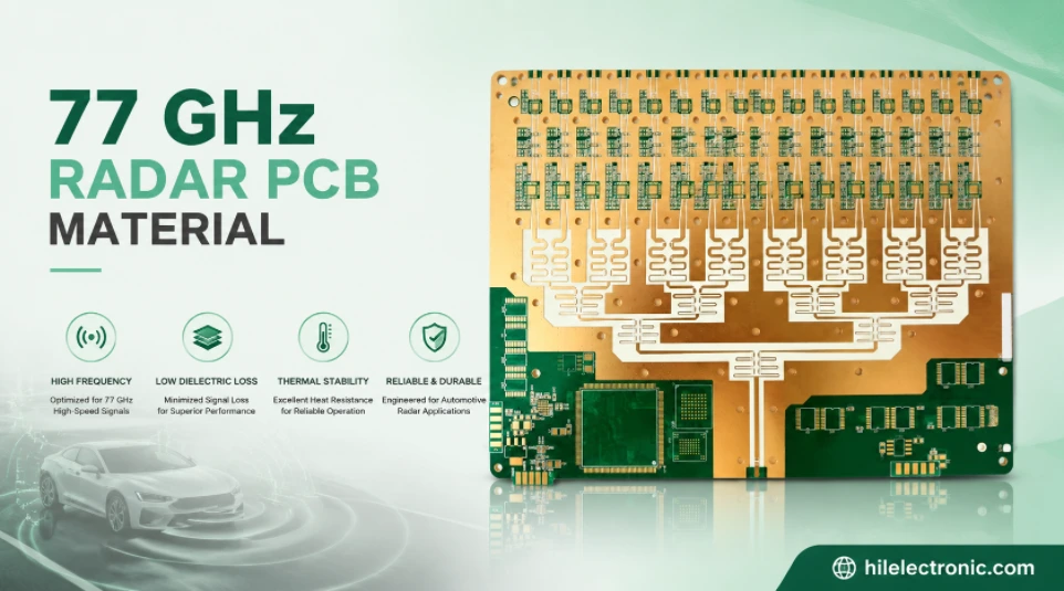
77 GHz Radar PCB Material Selection and Manufacturing Guide
Table of contentsWhat 77 GHz Changes in a PCBCommon 77 GHz...
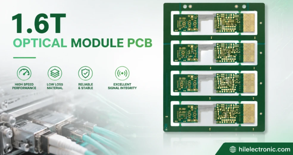
1.6T Optical Module PCB Manufacturing and Assembly Service
Table of contents1.6T Module Architectures and PCB...
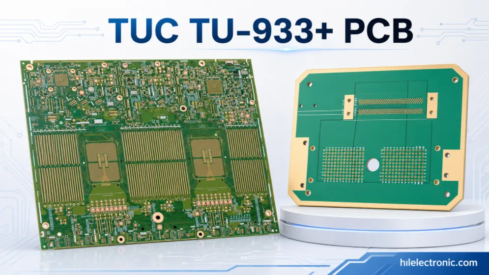
TUC TU-933+ PCB Manufacturing for Super-Low-Loss High-Speed Systems
Table of contentsWhat Is TU-933+ PCB Material?Why TU-933+...
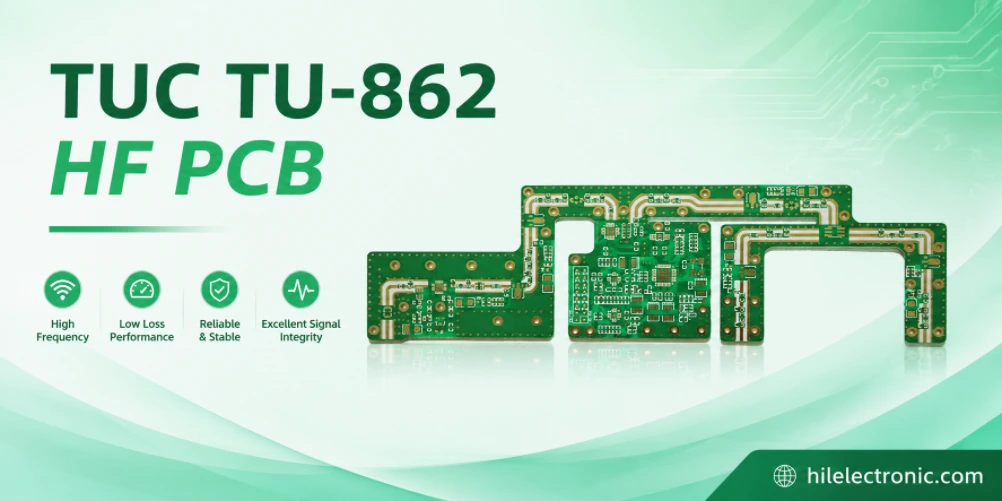
TUC TU-862 HF PCB Manufacturing and Assembly Service
Table of contentsWhat Is TU-862 HF?Why Choose TU-862 HF...
How to get a quote for PCBs
Let‘s run DFM/DFA analysis for you and get back to you with a report. You can upload your files securely through our website. We require the following information in order to give you a quote:
-
- Gerber, ODB++, or .pcb, spec.
- BOM list if you require assembly
- Quantity
- Turn time
In addition to PCB manufacturing, we offer a comprehensive range of electronic services, including PCB design, PCBA, and turnkey solutions. Whether you need help with prototyping, design verification, component sourcing, or mass production, we provide end-to-end support to ensure your project’s success.
For PCBA services, please provide your BOM (Bill of Materials) and any specific assembly instructions. We also offer DFM/DFA analysis to optimize your designs for manufacturability and assembly, ensuring a smooth production process.