
1.6T Optical Module PCB Manufacturing and Assembly Service
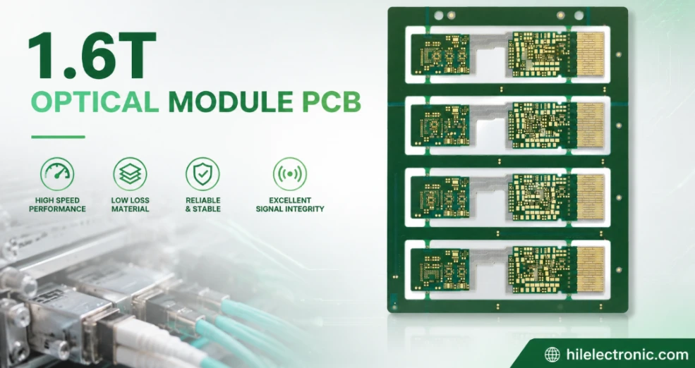
A 1.6T optical module PCB must carry next-generation high-speed electrical lanes in a tightly constrained module. OSFP can support 1.6 Tb/s with eight 200G-class electrical lanes, while OSFP-XD can reach 1.6 Tb/s using sixteen 100G-class lanes. The exact architecture determines the PCB, connector, channel and thermal requirements.
Highleap Electronics manufactures and assembles the PCB. We do not manufacture laminate, optical engines, lasers, DSPs or connectors. We process verified materials and approved components into the finished module PCBA.
Can Highleap manufacture a 1.6T optical module PCB? Yes, subject to 224G-class channel review, package escape, connector geometry, low-loss stackup, HDI, thermal design, assembly tooling and test requirements.
1.6T Module Architectures and PCB Impact
8 × 200G-class lanes
Fewer electrical lanes but much higher per-lane bandwidth, increasing loss and launch sensitivity.
16 × 100G-class lanes
More routing density, crosstalk management and connector pins in the module.
Retimed optics
DSP or retimer components add power, heat and high-density BGA escape.
Linear optics
Reduced retiming can lower power but places stricter requirements on the end-to-end electrical channel.
OIF’s current 224G work targets next-generation pluggable and linear optical applications. The PCB must be released against the applicable interface and form-factor documents, not a generic 1.6T label.
The practical outcome is a clear go/no-go decision: use the requested solution when the performance or compliance requirement needs it; choose a simpler approved construction when it does not. That judgement is made from the board and product data, not from the assumption that the highest specification always produces the best PCB.
A 1.6T module should not be released from the aggregate bandwidth figure alone. The electrical lane count and per-lane rate determine the connector pinout, DSP escape, number of high-speed layer pairs and allowable transition loss. A design based on more lanes at a lower lane rate can create different routing and power-distribution constraints from a design based on fewer, faster lanes. Highleap therefore reviews the actual architecture in the files before confirming the stackup or HDI route.
Primary 1.6T Optical Module PCB Challenges
- 224G-class channel loss: dielectric, copper, connector and via loss all become critical.
- Launch discontinuities: package and connector transitions require 3D field analysis and tight manufacturing control.
- Dense HDI escape: microvia geometry, capture pads and reference transitions must be reliable.
- Thermal concentration: advanced modules can dissipate substantial power in a small enclosure.
- Warpage and coplanarity: affect BGA soldering, optical alignment and mechanical fit.
- Test access: high-speed characterization requires planned coupons, fixtures and reference planes.
The purpose of the section is therefore both technical and commercial: explain why the issue matters, show how Highleap controls it, and give the buyer a simple path to start the review with the files already available.
This subject becomes useful when it is converted into a production decision. Highleap checks thermal density around the DSP and optical engine, 200G-class electrical lanes, very short but discontinuity-sensitive interconnects and HDI escape and via-in-pad structures, then records the agreed result in the stackup, process route and inspection plan. Purchasing receives a clear feasibility and quotation response rather than a theoretical explanation alone.
The difficulty is the interaction between constraints. Reducing trace length may force tighter package escape; adding copper for power delivery can disturb impedance or increase warpage; moving heat away from the DSP can conflict with optical-engine placement. These are not separate manufacturing questions. Our assigned engineer coordinates the high-speed, HDI, thermal and assembly reviews so that one improvement does not create a new failure elsewhere in the module.
Low-Loss Material, Copper and Glass Requirements
Material selection should be based on the actual 224G or 112G lane architecture. Ultra-low-loss thermoset systems, low-profile copper, low-Dk glass and controlled resin content may be needed. The selected construction must be purchasable and repeatable in production.
At these data rates, copper roughness and weave effects cannot be treated as secondary details. Highleap confirms the foil, glass style and stackup assumptions with the customer before CAM release.
Generic datasheet values are not enough when ordinary electrical testing cannot detect warpage around fine-pitch packages or assembly defects under via-in-pad BGAs. The review must use the exact core or prepreg, copper profile, finished thickness and via route. This is where one-to-one engineering support prevents the buyer from having to interpret multiple supplier documents alone.
The output of the review should be a buildable stackup and a short list of controlled variables. Highleap documents the agreed material identity, geometry, process route and inspection basis, then coordinates the remaining details internally across CAM, fabrication, quality and assembly.
1.6T Module Stackup and HDI Design
| Area | Design objective | Production control |
|---|---|---|
| SerDes escape | Short, symmetric transitions | Laser-via registration, filled via-in-pad and pad control |
| Connector region | Low return loss and crosstalk | Anti-pad geometry, reference stitching and profile accuracy |
| High-speed routes | Low loss, low skew and consistent impedance | Material, copper, glass, etch and thickness control |
| Power planes | Low impedance and heat spreading | Copper balance, thermal vias and plane integrity |
| Optical engine | Mechanical and electrical alignment | Datum, component placement and fixture control |
Repeatability is the main manufacturing test. A prototype can work even when the process window is broad, but volume production exposes variation in material lots, copper distribution, panel loading and plating. We place impedance and loss coupon planning, production stackup correlation, laser-drill and filled-via control and connector and package datum inspection in the production release to provide a stable comparison between lots.
The technical variables in this section cannot be evaluated independently. A change in thermal density around the DSP and optical engine can alter the effect of 200G-class electrical lanes, while very short but discontinuity-sensitive interconnects and HDI escape and via-in-pad structures influence the geometry and test result seen on the finished board. Highleap reviews the actual production construction so the stackup and compensation are based on purchasable materials rather than nominal examples.
What Happens When 1.6T Is Treated as an 800G Board with Faster Parts?
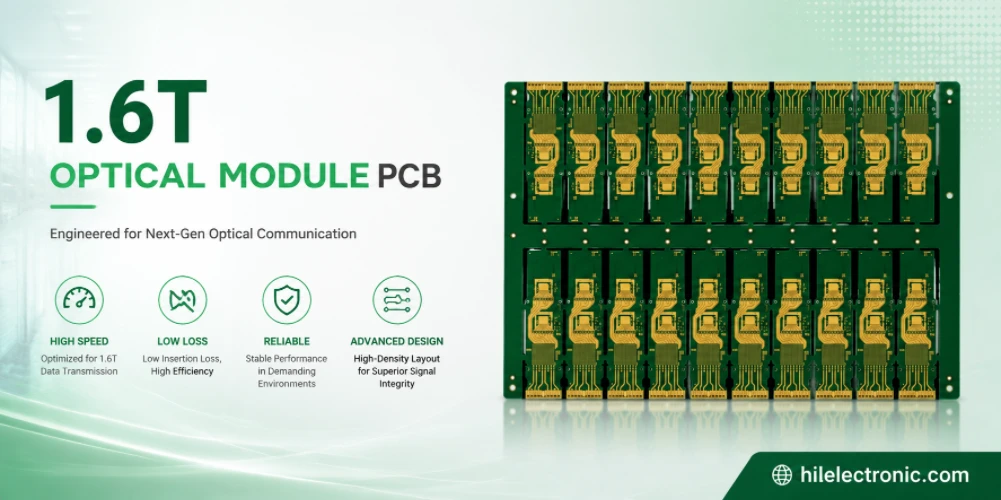
The risk is architectural, not incremental. Per-lane bandwidth, Nyquist frequency, connector behavior, package escape and thermal power change. Reusing an 800G stackup without new channel analysis can cause insertion-loss, return-loss, crosstalk, power-integrity and thermal failures.
Likewise, changing only to a lower-Df material does not solve a poor launch, excessive via stub or weak reference transition.
A broad response such as tightening every tolerance is usually wasteful. The correct action depends on whether the dominant cause is very short but discontinuity-sensitive interconnects, HDI escape and via-in-pad structures, thermal density around the DSP and optical engine or 200G-class electrical lanes. Targeted controls improve yield and make the root cause traceable without turning the entire drawing into an unnecessarily expensive special process.
These risks should lower the effort required to contact the factory, not raise it. Once Highleap receives the Gerber or design files, we check production stackup correlation, laser-drill and filled-via control, connector and package datum inspection and impedance and loss coupon planning. Only decisions that materially affect function, compliance, price or delivery are returned to the customer.
Highleap 1.6T Optical Module PCB Manufacturing
Highleap supports low-loss and ultra-low-loss multilayers, HDI, sequential lamination, laser drilling, filled via-in-pad, back drilling, fine-line imaging, controlled impedance, profile control and optional high-frequency coupon testing. Process flow is released only after reviewing the package, stackup and channel constraints.
A capability claim has value only when it is connected to a controlled shop-floor route. Highleap links production stackup correlation, laser-drill and filled-via control, connector and package datum inspection and impedance and loss coupon planning to incoming inspection, lamination, drilling, plating, imaging and final verification. The exact sequence remains subject to the approved material and board construction.
Different designs require different process windows. Board thickness, material chemistry, copper balance, hole architecture and panel size can change preparation, pressing and plating conditions. The assigned engineer coordinates CAM, production and quality so the customer receives one manufacturing answer instead of separate questions from each department.
Precision Assembly for 1.6T Modules
Assembly services include SPI, fine-pitch placement, BGA/LGA reflow, AOI, X-ray, connector and shield installation, thermal-interface materials, programming and customer-defined functional tests. Specialized optical alignment, laser handling or active optical test requires the customer’s approved fixtures, work instructions and acceptance criteria.
Thermal and warpage planning
Stencil design, reflow profile, board support, copper balance, component placement and heat-spreader installation are reviewed together. Rework limits should be defined before NPI.
Rework limits must be considered before production. Repeated thermal exposure can damage pads, laminate or moisture-sensitive components, especially around very short but discontinuity-sensitive interconnects and HDI escape and via-in-pad structures. The assembly review therefore addresses stencil, profile, component handling and inspection before defining an acceptable repair route.
Rework limits must be considered before production. Repeated thermal exposure can damage pads, laminate or moisture-sensitive components, especially around HDI escape and via-in-pad structures and thermal density around the DSP and optical engine. The assembly review therefore addresses stencil, profile, component handling and inspection before defining an acceptable repair route.
1.6T PCB Test and Qualification
Bare-board acceptance can include electrical test, impedance, microsection, dimensional inspection and representative S-parameter or insertion-loss coupons. Module-level compliance requires specialized instruments and fixtures.
Highleap can build compliance boards or test coupons to customer data, but cannot infer a compliance mask from the product name. The frequency range, reference impedance, port definition, de-embedding and pass/fail criteria must be supplied.
A coupon must represent the feature being controlled. Layer pair, copper, dielectric thickness, routing geometry and panel position should correspond to the critical circuit. Our engineers confirm whether a standard impedance coupon is sufficient or whether a dedicated loss, resonator or customer test structure is needed.
The release should state how an out-of-limit result will be investigated. Material records, dimensions, cross-section, plating data and assembly inspection may all be needed. A defined escalation path makes the test actionable rather than collecting measurements with no agreed production response.
Begin the 1.6T PCB Review with Gerber or PCB Design Files
A 1.6T project is technically demanding, but the first contact should be simple. Send the Gerber files or original PCB design files. If the fabrication notes are already included, no additional manufacturing document is required at this stage.
Your engineer connects you with the right specialists
Highleap assigns an engineer to work with you directly and coordinate the review with our high-speed PCB, HDI and assembly teams. We will examine the lane architecture, connector region, material, vias, thermal constraints and PCBA scope, then request only the information needed for feasibility and quotation. Assembly and test files can be added as the project review progresses.
Purchasing is not expected to complete a signal-integrity, RF or lamination questionnaire before contacting us. After reviewing the board files, we ask focused questions about thermal density around the DSP and optical engine, 200G-class electrical lanes, very short but discontinuity-sensitive interconnects or HDI escape and via-in-pad structures only when they change feasibility, price, delivery or acceptance.
1.6T Module PCB Cost and Schedule Drivers
Ultra-low-loss material, low-profile copper, multiple HDI cycles, filled microvias, tight profile tolerances, high-speed coupons, special connectors, advanced BGAs and test equipment drive cost. Material and component availability can dominate schedule. A firm quotation requires a released architecture.
Yield must be considered from prototype through volume. Features associated with excess return loss at launches or warpage around fine-pitch packages can increase scrap, rework and component loss. A stable documented construction usually has a lower total cost than an aggressive design that needs repeated changes after assembly.
The quotation reflects the complete route required to achieve acceptable yield. Major drivers include ultra-low-loss material, low-profile copper, sequential lamination, filled microvias, fine geometry, inspection and test coverage. Material price is only one component; extra lamination, special drilling, tight registration, inspection time and test coupons can have an equal or larger effect.
A 1.6T Module Requires Co-Engineering Across PCB and PCBA
The board, connector, package, optical engine, thermal design and manufacturing process are tightly coupled. Highleap provides the PCB fabrication and assembly path while respecting the material supplier and component supplier roles.
Customers do not need to complete that engineering package before making contact. Gerber or PCB design files are enough to begin. The assigned engineer organizes the review, explains the decisions that require approval and coordinates fabrication, component sourcing, assembly and testing.
The finished board must be released as one electrical, mechanical and manufacturing system. Highleap connects the customer files with connector and package datum inspection, impedance and loss coupon planning, production stackup correlation and the agreed inspection method. That documentation allows a successful prototype to be repeated when volume increases or the order returns later.
Frequently Asked Questions
Is every 1.6T optical module based on eight 224G electrical lanes?
No. Architecture depends on form factor and implementation; OSFP and OSFP-XD can reach 1.6T with different lane counts.
Does Highleap manufacture optical engines or low-loss laminate?
No. We manufacture PCBs and PCBAs using approved materials and sourced or consigned components.
Can you build 224G-capable module PCBs?
Yes, subject to channel, stackup, connector, HDI and test review.
Are HDI and via-in-pad required?
Often, but not universally. The package pitch and escape architecture determine the structure.
What files are needed to begin a 1.6T optical module PCB review?
Send the Gerber files or native PCB design files first. If fabrication notes are included, that is enough to begin. A Highleap engineer will coordinate any additional PCB, assembly or test information with you.
What information is needed before material selection?
Lane rate, reach, channel loss budget, connector, package, stackup space, thermal design and qualification constraints.
Technical reference note: Material properties and interface descriptions must be checked against the current manufacturer datasheet, customer specification and applicable interface standard for the exact production construction. Highleap Electronics is the PCB fabrication and PCB assembly provider; laminate and component trademarks belong to their respective manufacturers.

Recommended Posts

Taconic RF 35 vs RO4350B PCB
Table of contentsRF-35 vs RO4350B Procurement and...

TMM4 Filter PCB Manufacturing
TMM4 filter PCB manufacturing is controlled by the...

TMM3 PCB Manufacturing for RF Modules
TMM3 PCB manufacturing is most useful where the RF module...

TMM6 PCB Fabrication
TMM6 fabrication is the process-control page for a mid-Dk...
How to get a quote for PCBs
Let’s run DFM/DFA analysis for you and get back to you with a report. You can upload your files securely through our website. We require the following information in order to give you a quote:
-
- Gerber, ODB++, or .pcb, spec.
- BOM list if you require assembly
- Quantity
- Turn time
For PCBA services, please provide your BOM (Bill of Materials) and any specific assembly instructions. We also offer DFM/DFA analysis to optimize your designs for manufacturability and assembly, ensuring a smooth production process.